
Data Sheet


PmodISNS20™ Reference Manual
Copyright Digilent, Inc. All rights reserved.
Other product and company names mentioned may be trademarks of their respective owners.
Page 2 of 3
2 Interfacing with the Pmod
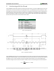
The PmodISNS20 communicates with the host board via the SPI protocol. The 12 bits of digital data are sent to the
system board in 16 clock cycles with the most significant bit first. For the ADC7476, each bit is shifted out on each
falling edge of the serial clock line after the chip select line is brought low with the first four bits as leading zeroes
and the remaining 12 bits representing the 12 bits of data. The datasheet for the ADC7476 recommends that for
faster microcontrollers or DSPs, the serial clock line is first brought to a high state before being brought low after
the fall of the chip select line to ensure that the first bit is valid.
Header J1
Pin
Signal
Description
1
CS
Chip Select
2
(NC)
Not Connected
3
MISO
Master-In-Slave-Out
4
CLK
Serial Clock
5
GND
Power Supply Ground
6
VCC
Positive Power Supply (3.3V)
Table 1. Pinout description table.
Figure 1. PmodISNS20 timing diagram.
The PmodISNS20 uses three wires to communicate with the host board. The wires used are Chip Select (CS), Serial
Clock (CLK), and Data Out (DO) – also known as MISO. At 0.0 Amps, the ADC will return over SPI a value of 2048. At
full negative current, a value of 0 will be returned, and likewise at full positive current a value of 4095 will be
returned. Knowing this we can derive the equation needed in order to convert this signal into useful information.