
Data Sheet

Pmod CMPS2™ Reference Manual
Copyright Digilent, Inc. All rights reserved.
Other product and company names mentioned may be trademarks of their respective owners.
Page 3 of 12
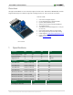
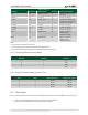
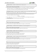
1.1 Pinout Table Diagram
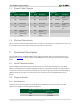
Header J1
Header J2
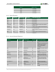
Jumper JP1
Pin
Signal
Description
Pin
Signal
Description
Pin
Status
Description
1
N/C
Not Connected
1
N/C
Not Connected
SCL
Loaded
4.7 kΩ Pullup
to Vcc
2
N/C
Not Connected
2
N/C
Not Connected
SCL
Unloaded
No Pullup to
Vcc
3
SCL
Serial Clock
3
SCL
Serial Clock
SDA
Loaded
4.7 kΩ Pullup
to Vcc
4
SDA
Serial Data
4
SDA
Serial Data
SDA
Unloaded
No Pullup to
Vcc
5
GND
Power Supply
Ground
5
GND
Power Supply
Ground
6
VCC
Power Supply
(3.3V)
6
VCC
Power Supply
(3.3V)
1.2 Physical Dimensions
The pins on the pin header are spaced 100 mil apart. The PCB is 1.25 inches long on the sides parallel to the pins on
the pin header and 0.8 inches long on the sides perpendicular to the pin header.
2 Functional Description
The Pmod CMPS2 utilizes the MMC34160PJ to collect magnetic field data. While communicating with the host
board via the I²C protocol using an I²C address of 0x0110000/ users can measure the ±16 G field surrounding the
device.
2.1 Serial Communication
The Pmod CMPS2 communicates with the host board via the I²C protocol. By first sending the 7-bit I²C device
address of 0110000 and then a read/write bit (high/low logic level, respectively), followed by the register address
of interest at a maximum clock frequency of 400 kHz users can both configure and read from the Pmod CMPS2. An
additional set of pins on header J2 is provided so that users may daisy chain the Pmod CMPS2 with other I²C
devices.
2.2 Register Details
2.2.1 Data Registers
Each Cartesian axis has two registers to store the high and low data bytes for each measurement. The data
registers are arranged in a low byte, high byte arrangement.
Data Registers addresses 0x00 to 0x05
Address
Register Name
0x00
X out LSB
0x01
X out MSB