
Data Sheet

Nexys Video™ FPGA Board Reference Manual
Copyright Digilent, Inc. All rights reserved.
Other product and company names mentioned may be trademarks of their respective owners.
Page 8 of 29
before programming, and then allowing the FPGA to decompress the bitstream itself during configuration.
Depending on design complexity, compression ratios of 10x can be achieved. Bitstream compression can be
enabled within the Xilinx tools (ISE or Vivado) to occur during generation. For instructions on how to do this,
consult the Xilinx documentation for the toolset being used. This option is available for all programming modes.
Mode-specific speed-ups are also available. JTAG clock frequency can be set to the maximum supported by the
programming cable in iMPACT/Vivado Hardware Manager. Similarly, the clock frequency for the SPI Flash can be
increased in device properties (Vivado) or bitstream generation options (ISE). The microSD and USB mass-storage
device configuration modes already operate at their maximum possible speed.
After being successfully programmed, the FPGA will illuminate the "DONE" LED. Pressing the "PROG" button at any
time will reset the configuration memory in the FPGA. After being reset, the FPGA will immediately attempt to
reprogram itself from whatever method has been selected by the programming mode jumpers.
The following sections provide greater detail about programming the Nexys Video using the different methods
available.
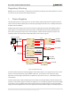
2.1 JTAG Programming
The Xilinx tools typically communicate with FPGAs using the Test Access Port and Boundary-Scan Architecture,
commonly referred to as JTAG. During JTAG programming, a .bit file is transferred from the PC to the FPGA using
the onboard Digilent USB-JTAG circuitry (port J12) or an external JTAG programmer, such as the Digilent JTAG HS2,
attached to port J17. You can perform JTAG programming at any time after the Nexys Video has been powered on,
regardless of what the mode jumper (JP4) is set to. If the FPGA is already configured, then the existing
configuration is overwritten with the bitstream being transmitted over JTAG. Setting the mode jumper to the JTAG
setting is useful to prevent the FPGA from being configured from any other bitstream source until a JTAG
programming occurs.
Programming the Nexys Video with an uncompressed bitstream using the on-board USB-JTAG circuitry usually
takes around four seconds with a 30 MHz JTAG clock.
JTAG programming can be done using the hardware server in Vivado or the iMPACT tool included with ISE. The
Nexys Video Programming Guide available on the Nexys Video Resource Center walks through the process of
building a bitstream and using it to program the Nexys Video.
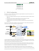
2.2 Quad-SPI Programming
For the FPGA to be able to configure itself from the SPI Flash, it first needs to be programmed with the bitstream.
This is called indirect programming and is a two-step process controlled by Hardware Manager (Vivado) or iMPACT
(ISE). First, the FPGA is programmed with a design that can program flash devices, and then data is transferred to
the flash device via the FPGA circuit (this complexity is hidden from the user by the Xilinx tools). After the flash
device has been programmed, it can automatically configure the FPGA at a subsequent power-on or reset event as
determined by the mode jumper setting. Programming files stored in the flash device will remain until they are
overwritten, regardless of power-cycle events.
Programming the flash can take as long as four to five minutes, which is mostly due to the lengthy erase process
inherent to the memory technology. Once written however, FPGA configuration can be very fast; taking less than a
second. Bitstream compression, SPI bus width, and configuration rate are factors controlled by the Xilinx tools that
can affect configuration speed. The on-board flash has a Quad-SPI interface, which supports single (x1), dual (x2),
and quad (x4) modes. The quad mode results in the fastest possible data transfer rate. In order for the quad mode