
Data Sheet

Nexys Video™ FPGA Board Reference Manual
Copyright Digilent, Inc. All rights reserved.
Other product and company names mentioned may be trademarks of their respective owners.
Page 6 of 29
12P0V pin of the FMC connector, the battery voltage must be 12VDC ±5 % in FMC applications, the same as the
wall supply specification. In any case, 15V is an absolute maximum.
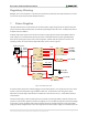
Voltage regulator circuits from Analog Devices® create the different voltages required by the FPGA and on-board
peripherals from the main power input. Some regulators use the outputs of another regulator as input, depending
on design considerations. In some cases, this chaining helps in creating the proper power-on sequence for circuits.
In other cases, the chaining of power supply enables achieves the same purpose.
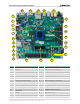
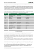
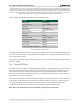
Table 1 provides information on maximum and typical currents for each power rail. The typical currents strongly
depend on FPGA configuration and the values provided represent medium size/speed designs.
Supply
Circuits
Device
Current (max/typical)
3.3 V
FPGA I/O, USB, FMC, Clocks,
Pmod, Ethernet, SD slot,
Flash, DisplayPort
IC26: ADP5052
4A / 0.1 to 1.5A
1.0 V
FPGA Core
IC26: ADP5052
4A / 0.2 to 2A
1.8 V
FPGA Auxiliary
IC26: ADP5052
1.2A / 0.15A
1.5 V
DDR3 and FPGA I/O
IC26: ADP5052
1.2 A / 0.5 A
2.5 V
FPGA I/O and Ethernet
IC26: ADP5052
0.2 A / 0.1 A
V
ADJ
(1.2-3.3 V)
User I/O, FMC, and FPGA I/O
IC28: ADP2384
2 A / 0.1 A
3.3 V
Audio analog supply
IC6: ADP150
0.15 A / 0.05 A
5.0 V
USB Host, HDMI
IC30: ADP2370
0.8 A / 0.5 A
MGT 1.0 V
Gigabit Transceivers VCC
IC31: ADP123
0.3 A
MGT 1.2 V
Gigabit Transceivers VTT
IC33: ADP123
0.3 A
XADC 1.8 V
XADC supply
IC34: ADP123
0.3 A
XADC 1.25 V
XADC reference
IC32: ADR127
5 mA
Table 1. Voltage rail power ratings.
The V
ADJ
power rail requires special attention. It is a programmable voltage rail that powers the FMC mezzanine
connector, user push-buttons, switches, XADC Pmod connector, and the FPGA banks connected to these
peripherals (banks 15, 16). The feedback pin of the V
ADJ
regulator is connected to an analog multiplexer controlled
by two FPGA signals, "SET_VADJ(1:0)". The multiplexer is able to change the resistor values in the feedback loop,
thereby changing the voltage on the regulator's output. Depending on the value set on the "SET_VADJ(1:0)" pins,
the possible voltages are listed in
Table 2. The third control pin is the "VADJ_EN" signal, which can disable the regulator altogether. If these control
pins are not used in the FPGA design, on-board pull resistors enable the regulator and set the V
ADJ
voltage to 1.2 V.
An FPGA design can dynamically change the V
ADJ
voltage to suit a certain FMC mezzanine card or application. Care
must be taken to disable the regulator first by bringing "VADJ_EN" low, setting "SET_VADJ(1:0)" and enabling the
regulator again. Please note that for proper voltage levels in digital signals connected to V
ADJ
-powered FPGA banks
(ex. user push-buttons), the correct I/O standard still needs to be set in the design user constraints (XDC or UCF
file). See the schematic and/or the constraints file to determine which signals are in V
ADJ
-powered banks. The
provided master UCF and XDC files assume the default V
ADJ
voltage of 1.2V, declaring LVCMOS12 as the I/O
standard for these signals.