
Data Sheet

Nexys Video™ FPGA Board Reference Manual
Copyright Digilent, Inc. All rights reserved.
Other product and company names mentioned may be trademarks of their respective owners.
Page 29 of 29
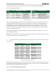
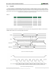
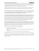
ADAU1761
Artix-7
ADC_SDATA
LRCLK
DAC_SDATA
BCLK
MCLK
T4
W6
T5
U5
U6
SDA
V5
SCL
W5
L/RHP
L/ROUTP
L/RAUX
L/RINN
Headphone Out
Line Out
Line In
Microphone In
Figure 16. Audio signal connections.
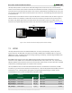
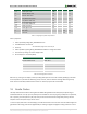
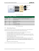
Signal Name
FPGA Pin
Pin Function
ADC_SDATA
T4
Serialized audio resulting from the analog-to-digital conversion (record).
DAC_SDATA
W6
Serialized audio is converted to analog by the codec (playback).
BCLK
T5
Serial data port clock.
LRCLK
U5
Serial data port frame clock.
MCLK
U6
Master clock.
SDA
V5
I
2
C configuration interface.
SCL
W5
I
2
C configuration interface.
Table 13. Audio signal description.
17 Out-of-box Demo
The Nexys Video comes with an out-of-box demo design that gets loaded from the on-board Quad SPI flash. It
exercises most of the on-board peripherals. Follow the instructions to explore them all:
Connecting an HDMI/DVI or DisplayPort monitor shows a test pattern with a mouse pointer.
Connecting a USB mouse controls the mouse pointer on the display.
Connecting an HDMI/DVI source, like a laptop output, replaces the test pattern with the source image.
Connecting the board to an Ethernet network will acquire link, IP address, and become "pingable" at the
IPv4 address displayed on the OLED.
The internal XADC temperature is read and shown on the OLED.
Connecting the USB-UART port to a PC and opening a terminal (115200,8,N,1) shows status messages.
Pushing BTNU records audio off the microphone input for five seconds and plays it back on the
headphone output if BTND is pushed, or line-out if BTNL. Similarly, BTNR starts a recording off the line-in
jack.
Slide switches are wired to the LEDs above.
The source code for this design is available on the Nexys Video Resource Center.