
Data Sheet

Nexys Video™ FPGA Board Reference Manual
Copyright Digilent, Inc. All rights reserved.
Other product and company names mentioned may be trademarks of their respective owners.
Page 28 of 29
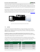
at up to 24 bits and 96 kHz sampling rate. Digital audio data is carried to/from the FPGA on a serial, full-duplex
interface which supports several different formats, the default being I
2
S. This interface is clocked by the FPGA
through BCLK by default, but the codec can be configured to provide the clock itself.
Configuring the audio codec can be done over I
2
C. It responds to slave address 0b0111011, followed by a 16-bit
register address and one or more data bytes. These registers control every functional aspect of the codec.
The codec is clocked from the FPGA through the Master Clock (MCLK) pin. A clock must be provided for the codec
to function, including the I
2
C port. The exact frequency depends on the desired sample rate and whether PLL will
be used, but 12 MHz is a good start. The clocking infrastructure of a 7 series FPGA is more than capable of
synthesizing the right frequency from the on-board 100 MHz reference oscillator.
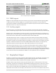
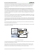
For proper use, the concept of audio paths needs to be understood. There are two signal paths internal to the
codec: Playback and Record. Both are highly configurable analog paths with mixers and amplifiers that route audio
signals through the chip. The Playback path is the output path that routes audio from different sources, like the
digital-to-analog converter or input mixers towards the headphone and line-out jacks. On the other hand, the
record path routes audio from the line-in and microphone-in towards the analog-to-digital converters. Having
routing elements at every step enables signal mixing between channels, amplification, muting, and bypass.
However, it also means that each element has to be properly configured along the path.
Keep in mind that audio jack designations might differ from codec analog frontend designators. For example, the
line-in jack connects to the AUX port of the codec. The microphone jack is wired to the IN port. Also, notice that
although some ports offer differential amplifiers and signaling, they are not used on the Nexys Video. For example,
the OUT port is differential, comprising 4 pins: LOUTP, LOUTN, ROUTP, and ROUTN. However, the N-side of the
differential pairs is left floating, while the P-side connects to the jack.
At the very least, an audio-aware FPGA design should do the following:
1. Provide MCLK for the audio codec.
2. Use an I
2
C master controller to configure the core clocking, sample rates, serial interface format, and
audio path.
3. Send or receive audio samples over the serial audio data channel for playback or record.
A MicroBlaze-based reference project that uses the audio codec is available on the Nexys Video Resource Center.
More advanced users might want to try additional features of the ADAU1761. For example, the on-chip SigmaDSP
core can be programmed to do user-defined digital signal processing. All relevant information can be found in the
ADAU1761 data sheet.