
Data Sheet

Nexys Video™ FPGA Board Reference Manual
Copyright Digilent, Inc. All rights reserved.
Other product and company names mentioned may be trademarks of their respective owners.
Page 27 of 29
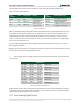
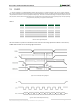
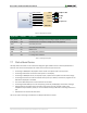
Symbol
Parameter
Min
Typ.
Max
Unit
t
cycle
Clock Cycle Time
100
-
-
ns
t
AS
Address Setup Time
15
-
-
ns
t
AH
Address Hold Time
15
-
-
ns
t
CSS
Chip Select Setup Time
20
-
-
ns
t
CSH
Chip Select Hold Time
10
-
-
ns
t
DSW
Write Data Setup Time
15
-
-
ns
t
DHW
Write Data Hold Time
15
-
-
ns
t
CLKL
Clock Low Time
20
-
-
ns
t
CLKH
Clock High Time
20
-
-
ns
t
R
Rise Time
-
-
40
ns
t
F
Fall Time
-
-
40
ns
Table 13. Timing diagram symbols and parameters.
Start-up sequence:
1. Power up VDD by pulling OLED_VDD low. Wait 1ms.
2. Pulse RES# low for at least 3us.
Send initialization/configuration commands (see
3. Table 12).
4. Power up VBAT by pulling OLED_VBAT low. Wait 100ms for voltage to stabilize.
5. Clear screen by writing zero to the display buffer.
6. Send "Display On" command (0xAF).
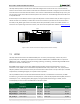
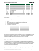
Command function
Command bytes
Charge pump enable
0x8D, 0x14
Set pre-charge period
0xD9, 0xF1
Contrast control
0x81, 0x0F
Column inversion disable
0xA0
Scan direction
0xC0
COM pins configuration
0xDA, 0x00
Addressing mode: horizontal
0x20
Table 12. OLED configuration commands.
After start-up, writing to the display is done by sending data bytes over the serial interface (D/C# high). Each data
bit corresponds to a pixel with the addressing mode, inversion, and scan direction settings determining exactly
which. Check out the Nexys Video Resource Center for reference projects that use the OLED.
16 Audio Codec
The Nexys Video board includes an Analog Devices ADAU1761 SigmaDSP audio codec (IC4) complementing its
multimedia features. Four 1/8" (3.5mm) audio jacks are available for line-out (J5-green), headphone-out (J3-black),
line-in (J7-blue), and microphone-in (J6-pink). Each jack carries two channels of analog audio (stereo), with the
exception of the microphone input, which is mono.
To record or play back audio in an FPGA design, the audio data needs to be converted. The audio codec bridges the
gap between the analog jacks and the digital FPGA pins. Analog-to-digital and digital-to-analog conversion is done