
Data Sheet


Nexys Video™ FPGA Board Reference Manual
Copyright Digilent, Inc. All rights reserved.
Other product and company names mentioned may be trademarks of their respective owners.
Page 25 of 29
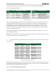
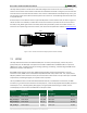
The auxiliary channel is a bidirectional channel for link management and device control. It is AC-coupled, just like
the main link lanes, but uses a different encoding and the lower data rate of 1Mbps. Upon hot-plug detection, a
Source will attempt to configure the link through link training. Handshaking link parameters happens via the
auxiliary channel.
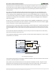
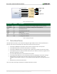
Nexys Video includes a Mini DisplayPort (mDP) connector wired in the Source role. The maximum lane count
supported is two. The two lanes of the main link are wired to the only gigabit transceiver bank: MGT bank 216.
Lane 0 is mapped to GTPE2_CHANNEL_X0Y4, while Lane 1 goes to GTPE2_CHANNEL_X0Y5. It is important to keep
in mind that bank 216, being the only one available in this FPGA package, is shared between the DisplayPort source
and FMC ports. Depending on the exact application, simultaneous usage of the FMC gigabit lane and DisplayPort
might not be possible.
On-board there is a 135 MHz reference oscillator mapped to GTPE2_COMMON_X0Y1/MGTREFCLK1, which should
be used to generate the desired link rate. Refer to the Xilinx "7 Series FPGAs GTP Transceivers User Guide" (ug482)
for more information on how to implement high-speed interfaces.
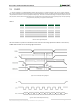
The auxiliary channel is a bidirectional LVDS bus. Depending on the Xilinx tool/IP version, instantiating a differential
I/O buffer with LVDS signaling standard might not be possible. The work-around is to have two pairs of pins wired
and shorted together, as seen in Figure 14. One pair should be implemented as input-only and the other as output-
only.
If the tool/IP allows bidirectional LVDS buffers, only one of the pairs needs to be used (it does not matter which),
while the other declared as input and not used.
The hot-plug detect (HPD) signal connects to a general user I/O pin and should be configured as an input. It will be
asserted when a sink is attached.
Artix-7
Lane 1
Lane 0
MGT 216
MGTTXP/N1
MGTTXP/N0
MGTREFCLK0P/N
Osc
135 MHz
AA9
AB10
AA10
AA11
AUX_P
AUX_N
N15
HPD
mDP
Figure 14. DisplayPort wiring diagram.
The full implementation details of the DisplayPort standard is outside the scope of this document. Refer to the full
specifications published by VESA for more details.
Xilinx provides a fully documented Vivado IP core that implements a DisplayPort controller. Using this core will
greatly decrease the development required to get DisplayPort working on the Nexys Video. This core requires a
paid license, but a 120 day evaluation license can be obtained for free from the Xilinx website.