
Data Sheet

Nexys Video™ FPGA Board Reference Manual
Copyright Digilent, Inc. All rights reserved.
Other product and company names mentioned may be trademarks of their respective owners.
Page 22 of 29
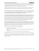
The Nexys Video provides a microSD slot for both FPGA configuration and user access. The on-board Auxiliary
Function microcontroller shares the SD card bus with the FPGA. Before the FPGA is configured, the microcontroller
must have access to the SD card via SPI interface. Once a bit file is downloaded to the FPGA (from any source), the
microcontroller powers off the SD slot and relinquishes control of the bus. The FPGA design will find the SD card in
an unpowered state.
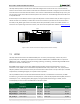
All of the SD pins on the FPGA are wired to support full SD speeds in native interface mode, as shown in Figure 13.
The SPI interface is also available, if needed. Once control over the SD bus is passed from the microcontroller to
the FPGA, the SD_RESET signal needs to be actively driven low by the FPGA to power the microSD card slot. For
information on implementing an SD card controller, refer to the SD card specification available at www.sdcard.org.
Artix-7
A1
SD MICRO (J3)
VDD
DAT2
DAT1
CMD
CLK
DAT3
DAT0
CARD_DETECT
3.3V
SD_RESET
C2
D2
B1
C1
E1
F1
E2
Figure 13. Artix-7 microSD card connector interface (PIC24 connections not shown).
13 HDMI
The Nexys Video board contains two buffered HDMI ports: one source port J8 (output), and one sink port J9
(input). Both ports use HDMI type-A receptacles and include an HDMI buffer: An AD8195 buffer for input and a
TMDS141 for output. The buffers work by terminating, equalizing, conditioning, and forwarding the HDMI stream
between the connector and FPGA pins.
Both HDMI and DVI systems use the same TMDS signaling standard, directly supported by Artix-7 user I/O
infrastructure. Also, HDMI sources are backward compatible with DVI sinks, and vice versa. Thus, simple passive
adaptors (available at most electronics stores) can be used to drive a DVI monitor or accept a DVI input. The HDMI
receptacle only includes digital signals, so only DVI-D mode is possible.
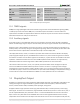
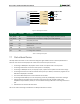
The 19-pin HDMI connectors include three differential data channels, one differential clock channel, five GND
connections, a one-wire Consumer Electronics Control (CEC) bus, a two-wire Display Data Channel (DDC) bus that is
essentially an I
2
C bus, a Hot Plug Detect (HPD) signal, a 5V signal capable of delivering up to 50mA, and one
reserved (RES) pin. All are wired to the FPGA with the exception of RES.
Pin/Signal
J8 (source)
J9 (sink)
Description
FPGA pin
Description
FPGA pin
D[2]_P, D[2]_N
Data output
AB3, AB2
Data input
U2, V2
D[1]_P, D[1]_N
Data output
AA1, AB1
Data input
W2, Y2
D[0]_P, D[0]_N
Data output
W1, Y1
Data input
Y3, AA3
CLK_P, CLK_N
Clock output
T1, U1
Clock input
V4, W4