
Data Sheet


Nexys Video™ FPGA Board Reference Manual
Copyright Digilent, Inc. All rights reserved.
Other product and company names mentioned may be trademarks of their respective owners.
Page 21 of 29
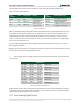
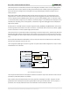
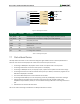
The on-board Pmod expansion connector labeled "JXADC" is wired to the auxiliary analog input pins of the FPGA.
Depending on the configuration, this connector can be used to input differential analog signals to the analog-to-
digital converter inside the Artix-7 (XADC). Any or all pairs in the connector can be configured either as analog
input or digital input-output.
The Dual Analog/Digital Pmod on the Nexys Video differs from the rest in the routing of its traces. The eight data
signals are grouped into four pairs, with the pairs routed closely coupled for better analog noise immunity.
Furthermore, each pair has a partially loaded anti-alias filter (100 ohm, 1 nF) laid out on the PCB. The filter does
not have capacitors C5, C8, C9, and C10. In designs where such filters are desired, the capacitors can be manually
loaded by the user.
NOTE: The coupled routing and the anti-alias filters might limit the data speeds when used for digital signals.
The XADC core within the Artix-7 is a dual channel 12-bit analog-to-digital converter capable of operating at 1
MSPS. Either channel can be driven by any of the auxiliary analog input pairs connected to the JXADC header. The
XADC core is controlled and accessed from a user design via the Dynamic Reconfiguration Port (DRP). The DRP also
provides access to voltage monitors that are present on each of the FPGA's power rails, and a temperature sensor
that is internal to the FPGA. For more information on using the XADC core, refer to the Xilinx document titled "7
Series FPGAs and Zynq-7000 All Programmable SoC XADC Dual 12-Bit 1 MSPS Analog-to-Digital Converter User
Guide" (ug480). A simple reference project that uses the XADC core can be found on the Nexys Video Resource
Center.
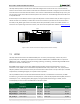
11 Low Pin Count FMC Connector
The Nexys Video includes an FPGA mezzanine card (FMC) standard-conforming carrier card connector that enables
connecting mezzanine modules compliant with the same standard. Nexys Video-based designs can now be easily
extended with custom or off-the-shelf high-performance modules.
The actual connector used is a Samtec ASP-134603-01, the low-pin count, 10mm stacking height variant of the
standard. It wires 34 differential pairs to regular FPGA user I/O pins powered by a voltage supply (V
ADJ
) adjustable
in the 1.2V-3.3V range. It also wires a 1 gigabit transceiver lane and its accompanying clock, the JTAG chain and
auxiliary signals, and various voltage rails required by the standard. Thanks to the flexible voltage range supported
by the Nexys Video, it allows high compatibility with existing and future FMC modules. It essentially allows the full
range of I/O standards supported by the Artix-7 I/O architecture over the FMC connector. The FPGA can even be
programmed to recognize the capabilities of a connected module and change the V
ADJ
voltage on-the-fly.
The pinout of the FMC connector can be found in the UCF/XDC constraints file available in the Nexys Video
Resource Center.
The gigabit transceiver lane includes a receive pair, a transmit pair, and a reference clock input to the FPGA, all
going to MGT bank 216. The transceiver lane is wired to lane 3 (GTPE2_CHANNEL_X0Y7). The reference clock is
wired to REFCLK1 of the same bank (GTPE2_COMMON_X0Y1). It is important to keep in mind that bank 216, being
the only one available in this FPGA package, is shared between the DisplayPort source and FMC ports. Depending
on the exact application, simultaneous usage of the FMC gigabit lane and DisplayPort might not be possible.
Regular FMC I/O signals are not affected.
12 MicroSD Slot