
Data Sheet

Nexys Video™ FPGA Board Reference Manual
Copyright Digilent, Inc. All rights reserved.
Other product and company names mentioned may be trademarks of their respective owners.
Page 10 of 29
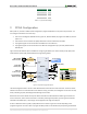
For proper operation of the memory, a memory controller and physical layer (PHY) interface needs to be included in the FPGA design. The Xilinx
in the FPGA design. The Xilinx 7 series memory interface solutions core generated by the memory interface generator (MIG) Wizard hides away
generator (MIG) Wizard hides away the complexities of a DDR3 interface. Depending on the tool used (ISE, EDK, or Vivado), the MIG Wizard can
Vivado), the MIG Wizard can generate a native FIFO-style or an AXI4 interface to connect to user logic. This workflow allows the customization
workflow allows the customization of several DDR3 parameters optimized for the particular application.
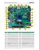
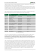
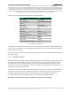
Table 3 below lists the MIG Wizard settings optimized for the Nexys Video.
Setting
Value
Memory type
DDR3 SDRAM
Max. clock period
2500ps (800Mbps data rate)
Clock ratio
4:1
Memory type
Components
Memory part
MT41K256M16HA-125
Memory voltage
1.5V
Data width
16
Data mask
Enabled
Input clock period
10000ps (100 MHz)
Output driver impedance
RZQ/6
Chip Select pin
Disabled
Rtt (nominal) – On-die termination
RZQ/6
Internal Vref
Enabled
Internal termination impedance
50ohms
Table 3. DDR3 settings for the Nexys Video.
The MIG Wizard will require the fixed pin-out of the memory signals to be entered and validated before generating
the IP core. For your convenience an importable UCF file and MIG .prj file is provided on the Nexys Video Resource
center to speed up the process.
For more details on the Xilinx memory interface solutions, refer to the "7 Series FPGAs Memory Interface Solutions
User Guide" (ug586).
3.2 Quad-SPI Flash
Non-volatile storage is provided by a Spansion S25FL256S flash memory. FPGA configuration files can be written to
flash memory, and mode settings are available to cause the FPGA to automatically read a configuration from this
device at power on. An Artix-7 200T configuration file requires just over 9 MiB (mebibyte) of memory, leaving
about 70% of the flash device available for user data. Or, if the FPGA is being configured from another source, the
whole memory can be used for custom data.
The contents of the memory can be manipulated by issuing certain commands on the SPI bus. The implementation
of this protocol is outside the scope of this document. All signals in the SPI bus, except SCK, are general-purpose
user I/O pins after FPGA configuration. SCK is an exception because it remains a dedicated pin even after
configuration. Access to this pin is provided through a special FPGA primitive called STARTUPE2.
NOTE: Refer to the manufacturer's data sheets and Xilinx user guides for more information.