300 Henley Court Pullman, WA 99163 509.334.6306 www.digilentinc.com Nexys Video™ FPGA Board Reference Manual Revised May 4, 2016 This manual applies to the Nexys Video rev. A Table of Contents Table of Contents .................................................................................................................. 1 Overview............................................................................................................................... 3 Regulatory Warning.........................
Nexys Video™ FPGA Board Reference Manual 8 9 USB HID Host ............................................................................................................... 15 8.1 HID Controller................................................................................................................. 15 8.2 Keyboard ........................................................................................................................ 16 8.3 Mouse..................................................
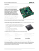
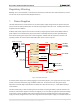
Nexys Video™ FPGA Board Reference Manual Overview The Nexys Video board is a complete, ready-to-use digital circuit development platform based on the latest Artix-7™ Field Programmable Gate Array (FPGA) from Xilinx®. With its large, high-capacity FPGA (Xilinx part number XC7A200T-1SBG484C), generous external memories, high-speed digital video ports, and 24-bit audio codec, the Nexys Video is perfectly suited for audio and video processing applications.
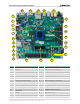
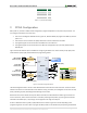
Nexys Video™ FPGA Board Reference Manual 26 25 24 23 22 1 21 2 3 20 4 19 5 4 18 6 7 17 8 16 4 9 15 10 11 13 12 14 Callout Component Description Callout Component Description 1 Power jack 14 MicroSD card slot (underneath) 2 Power Switch 15 Five pushbuttons 3 Power indicator LED 16 Miscellaneous XADC pins 4 Pmod Header(s) 17 Programming mode jumper 5 External fan control solder points 18 FMC header 6 FPGA programming done LED 19 FPGA configuration reset button 7
Nexys Video™ FPGA Board Reference Manual Regulatory Warning Warning: This is a class A product. In a domestic environment this product may cause radio interference, in which case the user may be required to take adequate measures. 1 Power Supplies The Nexys Video board can receive power from an external power supply through the center-positive barrel jack (J21) or the two-pin battery header (J22). The external supply voltage must be 12 V ±5 %. The Nexys Video cannot be powered from the USB bus.
Nexys Video™ FPGA Board Reference Manual 12P0V pin of the FMC connector, the battery voltage must be 12VDC ±5 % in FMC applications, the same as the wall supply specification. In any case, 15V is an absolute maximum. Voltage regulator circuits from Analog Devices® create the different voltages required by the FPGA and on-board peripherals from the main power input. Some regulators use the outputs of another regulator as input, depending on design considerations.
Nexys Video™ FPGA Board Reference Manual SET_VADJ(1:0) 00 (default) 01 10 11 VADJ 1.2 V 1.8 V 2.5 V 3.3 V Table 2. VADJ programmable voltages. 2 FPGA Configuration After power-on, the Artix-7 FPGA must be configured (or programmed) before it can perform any functions. You can configure the FPGA in one of four ways: 1. 2. 3. 4. A PC can use the Digilent USB-JTAG circuitry (port J12, labeled "PROG") to program the FPGA any time the power is on.
Nexys Video™ FPGA Board Reference Manual before programming, and then allowing the FPGA to decompress the bitstream itself during configuration. Depending on design complexity, compression ratios of 10x can be achieved. Bitstream compression can be enabled within the Xilinx tools (ISE or Vivado) to occur during generation. For instructions on how to do this, consult the Xilinx documentation for the toolset being used. This option is available for all programming modes.
Nexys Video™ FPGA Board Reference Manual to work, the bitstream needs to be generated with the x4 bus width option (Vivado device property) and the nonvolatile quad configuration bit in the flash needs to be enabled. The Nexys Video is shipped with this bit enabled. Indirect programming of the flash can also be done using the iMPACT tool included with ISE. The correct part to be set in the tools is s25fl256xxxxxx0 from the manufacturer Spansion®.
Nexys Video™ FPGA Board Reference Manual For proper operation of the memory, a memory controller and physical layer (PHY) interface needs to be included in the FPGA design. The Xilinx in the FPGA design. The Xilinx 7 series memory interface solutions core generated by the memory interface generator (MIG) Wizard hides away generator (MIG) Wizard hides away the complexities of a DDR3 interface.
Nexys Video™ FPGA Board Reference Manual SPI Flash Artix-7 CS# SDI/DQ0 SDO/DQ1 WP#/DQ2 HLD#/DQ3 SCK SPI Flash T19 P22 R22 P21 R21 L12/CCLK Figure 3. Nexys Video SPI Flash pin-out. 4 Ethernet PHY The Nexys Video board includes a Realtek RTL8211E-VL PHY paired with an RJ-45 Ethernet jack with integrated magnetics to implement a 10/100/1000 Ethernet port for network connection. The PHY interfaces with the FPGA via RGMII for data and MDIO for management. Bank 13 powered at 2.
Nexys Video™ FPGA Board Reference Manual with Xilinx part number EF-DI-TEMAC-PROJ or EF-DI-TEMAC-SITE. A free evaluation of this core is available; however, the design will stop working after running for approximately 8 hours. On an Ethernet network, each node needs a unique MAC address. To this end, a Microchip 24AA025E48 EEPROM is provided on the Nexys Video. On one hand, it is a read-writeable EEPROM that can be accessed via I2C.
Nexys Video™ FPGA Board Reference Manual driven by the 100 MHz input clock. For a full description of these rules and of the capabilities of the Artix-7 clocking resources, refer to the "7-Series FPGAs Clocking Resources User Guide" (ug472) available from Xilinx. Xilinx offers the Clocking Wizard IP core to help users generate the different clocks required for a specific design.
Nexys Video™ FPGA Board Reference Manual JTAG Micro-USB (J12) D0/SCK D1/MOSI D2/MISO D3/SS D4 D5 D6 D7 RXF# TXE# RD# WR# SIWU# OE# CLKOUT JTAG U20 P14 P15 U17 R17 P16 R18 N14 N17 Y19 P19 R19 P17 V17 Y18 FT2232H Artix-7 Figure 6. USB-FPGA interfaces provided by the USB PROG port. 7.1 Parallel Transfer Interface (DPTI) DPTI is an 8-bit wide parallel FIFO-style data interface that offers higher bandwidth than DSPI.
Nexys Video™ FPGA Board Reference Manual 7.2 Serial Peripheral Interface (DSPI) An industry-standard SPI interface can also be used for transferring data. It uses only four signals for serial fullduplex communication. The USB controller acts as a SPI master, with the FPGA taking the slave role. The USB controller initiates a transaction after API function calls are made and transfers data in both directions simultaneously.
Nexys Video™ FPGA Board Reference Manual first), odd parity, and stop bit, but the data packets are organized differently, and the keyboard interface allows bidirectional data transfers (so the host device can illuminate state LEDs on the keyboard). Bus timings are shown in Figure 8. Edge 0 Tck Tck Edge 10 CLOCK ‘0’ start bit Thld ‘1’ stop bit DATA Tsu Symbol Parameter Min Max 30us 50us TCK Clock time Data-to-clock setup time 5us 25us TSU THLD Clock-to-data hold time 5us 25us Figure 8.
Nexys Video™ FPGA Board Reference Manual Figure 9. Keyboard scan codes. A host device can also send data to the keyboard. Table 7 shows a list of some common commands a host might send. Command Action ED Set Num Lock, Caps Lock, and Scroll Lock LEDs. Keyboard returns FA after receiving ED, then host sends a byte to set LED status: bit 0 sets Scroll Lock, bit 1 sets Num Lock, and bit 2 sets Caps lock. Bits 3 to 7 are ignored. EE Echo (test).
Nexys Video™ FPGA Board Reference Manual The mouse assumes a relative coordinate system wherein moving the mouse to the right generates a positive number in the X field, and moving to the left generates a negative number. Likewise, moving the mouse up generates a positive number in the Y field, and moving down represents a negative number (the XS and YS bits in the status byte are the sign bits – a '1' indicates a negative number).
Nexys Video™ FPGA Board Reference Manual VADJ Buttons M17 BTNR M18 BTNU P18 BTND N17 BTNC LD0 H17 K15 J13 N14 R18 V17 U17 U16 P17 BTNL LD1 LD2 LD3 LD4 LD5 LD6 LD7 LEDs VADJ Slide Switches SW0 J15 SW1 L16 SW2 M13 SW3 R15 SW4 R17 SW5 T18 SW6 U18 SW7 R13 1.5V C12 BTN6 CPU Reset Artix-7 Figure 11. General purpose I/O connections.
Nexys Video™ FPGA Board Reference Manual The Nexys Video features four Pmod ports of different "styles" with subtle differences between them. Table 9 summarizes these differences. Pmod connector Power Analog/Digital JXADC VADJ Dual JA 3.3 V Digital-only JB, JC 3.3 V Digital-only Series protection Routing Differential; Pairs: 1-7,2-8,3-8,4-10 Single-ended Differential; Pairs: 1-2,3-4,7-8,9-10 100 ohm 200 ohm 0 ohm Recommended usage Analog inputs; LVDS_25 input/output (VADJ=2.
Nexys Video™ FPGA Board Reference Manual The on-board Pmod expansion connector labeled "JXADC" is wired to the auxiliary analog input pins of the FPGA. Depending on the configuration, this connector can be used to input differential analog signals to the analog-todigital converter inside the Artix-7 (XADC). Any or all pairs in the connector can be configured either as analog input or digital input-output. The Dual Analog/Digital Pmod on the Nexys Video differs from the rest in the routing of its traces.
Nexys Video™ FPGA Board Reference Manual The Nexys Video provides a microSD slot for both FPGA configuration and user access. The on-board Auxiliary Function microcontroller shares the SD card bus with the FPGA. Before the FPGA is configured, the microcontroller must have access to the SD card via SPI interface. Once a bit file is downloaded to the FPGA (from any source), the microcontroller powers off the SD slot and relinquishes control of the bus.
Nexys Video™ FPGA Board Reference Manual CEC Consumer Electronics Control bidirectional AA4 Consumer Electronics Control bidirectional AA5 SCL, SDA DDC bidirectional U3, V3 DDC bidirectional Y4, AB5 HPD/HPA Hot-plug detect input AB13 Hot-plug assert output AB12 5V0 Powered from 5V rail N/A Powers auxiliary signals N/A Transmitter enable output R3 TXEN Table 11. HDMI pin description and assignment. 13.
Nexys Video™ FPGA Board Reference Manual resulting in a packetized stream. This differentiates DisplayPort from other digital video standards, like DVI/HDMI. Due to the high link rate, the main link can only be implemented on dedicated gigabit transceiver pins of the Artix7 architecture. Copyright Digilent, Inc. All rights reserved. Other product and company names mentioned may be trademarks of their respective owners.
Nexys Video™ FPGA Board Reference Manual The auxiliary channel is a bidirectional channel for link management and device control. It is AC-coupled, just like the main link lanes, but uses a different encoding and the lower data rate of 1Mbps. Upon hot-plug detection, a Source will attempt to configure the link through link training. Handshaking link parameters happens via the auxiliary channel. Nexys Video includes a Mini DisplayPort (mDP) connector wired in the Source role.
Nexys Video™ FPGA Board Reference Manual 15 OLED A Univision Technology Inc. UG-2832HSWEG04 is loaded on the Nexys Video. It is a white monochrome, 128 x 32, 0.91" organic LED display 0.91" organic LED display matrix bundled with a Solomon Systech SSD1306 display controller. The display data interface towards the FPGA is a 4interface towards the FPGA is a 4-wire serial peripheral interface (SPI).
Nexys Video™ FPGA Board Reference Manual Symbol tcycle tAS tAH tCSS tCSH tDSW tDHW tCLKL tCLKH tR tF Parameter Clock Cycle Time Address Setup Time Address Hold Time Chip Select Setup Time Chip Select Hold Time Write Data Setup Time Write Data Hold Time Clock Low Time Clock High Time Rise Time Fall Time Min 100 15 15 20 10 15 15 20 20 - Typ. - Max 40 40 Unit ns ns ns ns ns ns ns ns ns ns ns Table 13. Timing diagram symbols and parameters. Start-up sequence: 1. 2. Power up VDD by pulling OLED_VDD low.
Nexys Video™ FPGA Board Reference Manual at up to 24 bits and 96 kHz sampling rate. Digital audio data is carried to/from the FPGA on a serial, full-duplex interface which supports several different formats, the default being I 2S. This interface is clocked by the FPGA through BCLK by default, but the codec can be configured to provide the clock itself. Configuring the audio codec can be done over I2C. It responds to slave address 0b0111011, followed by a 16-bit register address and one or more data bytes.
Nexys Video™ FPGA Board Reference Manual Artix-7 T4 W6 T5 U5 U6 V5 W5 L/RHP ADC_SDATA DAC_SDATA BCLK LRCLK MCLK SDA SCL L/ROUTP L/RAUX L/RINN Headphone Out Line Out Line In Microphone In ADAU1761 Figure 16. Audio signal connections. Signal Name FPGA Pin Pin Function ADC_SDATA T4 Serialized audio resulting from the analog-to-digital conversion (record). DAC_SDATA W6 Serialized audio is converted to analog by the codec (playback). BCLK T5 Serial data port clock.