
Data Sheet
10/3/2018 JTAG-SMT3-NC Reference Manual [Reference.Digilentinc]
https://reference.digilentinc.com/reference/programmers/jtag-smt3/reference-manual 5/16
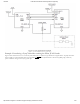
Small, complete, all-in-one JTAG programming/debugging solution for Xilinx FPGAs with UART side channel
Compatible with Xilinx Tools
High-Speed USB 2.0 port that can drive JTAG bus up to 30Mbit/sec (frequency settable by user)
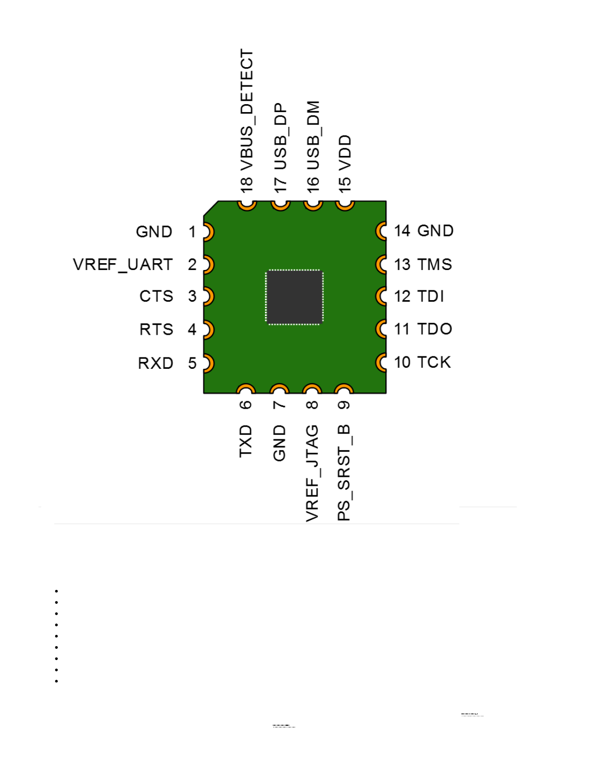
Open drain buffer on PS_SRST_B pin allows debugging software to reset the processor core of Xilinx’s Zynq® platform
Dual channel USB controller provides simultaneous access to both JTAG and UART interfaces
Separate Vref for JTAG and UART signals allows each interface to operate at difference voltages (1.8V to 5.5V)
Small form-factor surface-mount module can be directly loaded on target boards
USB D+ and D- signals routed to pads, allowing USB connector to be placed anywhere on the host PCB
VBUS_DETECT pin allows for reduced current consumption when the module isn’t connected to a PC
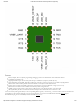
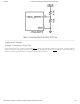
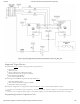
Users can connect JTAG signals directly to the corresponding FPGA signals, as shown in Fig. 1. For best results, mount the module over a
ground plane on the host PCB. Although users may run signal traces on top of the host PCB beneath the SMT3-NC (), Digilent
recommends keeping the area immediately beneath the SMT3-NC () clear.
Features