
Data Sheet
10/3/2018 JTAG-SMT3-NC Reference Manual [Reference.Digilentinc]
https://reference.digilentinc.com/reference/programmers/jtag-smt3/reference-manual 12/16
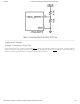
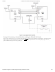
When possible, route DP and DM on the plane closest to the ground plane.
When possible, avoid routing the DP and DM signals through vias. If vias cannot be avoided, then keep them small and place the DP
and DM traces on the same layer.
When possible, avoid routing other traces near DP and DM.
When possible, minimize or avoid the use of bends in the DP and DM traces. If 90 degree bends are necessary, then use two 45
degree turns or an arc instead of a single 90 degree turn.
Do NOT route DP or DM near oscillators, crystals, switching regulators, clock generators, or inductors.
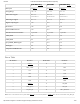
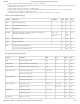
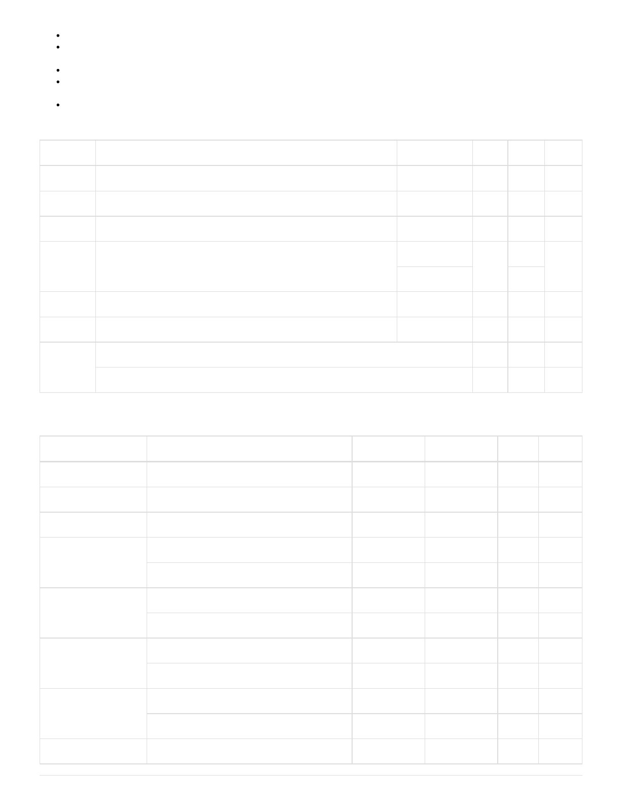
Symbol Parameter Condition Min Max Unit
Vdd Operating supply voltage -0.3 4.0 V
Vref I/O reference/supply voltage -0.3 6 V
VIO Signal Voltage -0.3 6 V
IIK,IOK TMS, TCK, TDI, TDO, TXD, RXD, RTS, CTS, PS_SRST_B
DC Input/Output Diode Current
VIO < -0.3V -50 mA
VIO > 6V +20
IOUT DC Output Current ±50 mA
TSTG Storage Temperature -10 +60 ºC
ESD Human Body Model JESD22-A114 4000 V
Charge Device Model JESD22-C101 2000 V
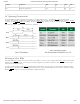
Symbol Parameter Min Typ Max Unit
Vdd Operating supply voltage 2.97 3.3 3.63 Volts
VREF_JTAG JTAG I/O reference/supply voltage 1.65 3.3 5.5 Volts
VREF_UART UART I/O reference/supply voltage 1.65 3.3 5.5 Volts
TDO, RXD, CTS Input High Voltage (VIH) 0.75 x Vref 5.5 Volts
Input Low Voltage (VIL) 0 0.55 Volts
VBUS_DETECT Input High Voltage (VIH) 2.0 Vdd Volts
Input Low Voltage (VIL) 0 0.8 Volts
TMS, TCK, TDI Output High (VOH) 0.78 x Vref 0.95 x Vref Vref Volts
Output Low (VOL) 0 0.05 x Vref 0.55 Volts
TXD, RTS Output High (VOH) 0.75 x Vref Vref Volts
Output Low (VOL) 0 0.55 Volts
PS_SRST_B Output Low (VOL) 0 0.55 Volts
Absolute Maximum Ratings
DC Operating Characteristics