
User Manual


EVB-USB3300-XLX User Manual
Revision 0.4 (06-29-07) SMSC EVB-USB3300-XLX
4
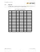
2.6 ULPI Signal Test Points
The headers J2, J3 and J4 provide easy access to the ULPI signals, and each pin has a silk screen
label as shown in Figure 1 .
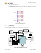
2.7 Block Diagram
The EVB-USB3300-XLX block diagram shows how the jumpers are used on the board.
Figure 1 ULPI Signal Test Points
Figure 2 EVB-USB3300-XLX Block Diagram
USB3300
J5
5V DC
Input
U1
VBUS
ID
DP
DM
USB OTG
Connector
24 MHz XTAL
3x13
Header
J6
J7
5.6uF 150uF
Install to source +5V
from the FPGA
development system.
VBUS Switch
500 mA current limit
w/ Fault Detection
ONA FAULTAn
VDD3.3
5V
EXTVBUS
CPEN
VDD3.3
ULPI Signals
DP
DM
ID
ULPI Bus
GND
J7 Install for
Host mode
J1