
Data Sheet

PmodLVLSHFT™ Reference Manual
Copyright Digilent, Inc. All rights reserved.
Other product and company names mentioned may be trademarks of their respective owners.
Page 2 of 3
Figure 1. Switches indicating the voltage direction.
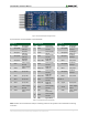
A pinout table for the PmodLVLSHFT is provided below:
Header J1
JTAG Header J2
Header J3
Pin
Signal
Description
Pin
Signal
Description
Pin
Signal
Description
1
AIO1/TMS
A1 & TMS
JTAG pin
1
GND
Power Supply
Ground
1
BIO1/TMS
B1 & TMS
JTAG pin
2
AIO2/TDI
A2 & TDI
JTAG pin
2
VCCB
Power Supply
side B
2
BIO5/SRST
B5 & Signal
Reset pin
3
AIO3/TDO
A3 & TDO
JTAG pin
3
GND
Power Supply
Ground
3
BIO2/TDI
B2 & TDI
JTAG pin
4
AIO4/TCK
A4 & TCK
JTAG pin
4
BIO1/TMS
B1 & TMS
JTAG pin
4
BIO6
I/O pin B6
5
GND
Power Supply
Ground
5
GND
Power Supply
Ground
5
BIO3/TDO
B3 & TDO
JTAG pin
6
VCCA
Power Supply
side A
6
BIO4/TCK
B4 & TCK
JTAG pin
6
BIO7
I/O pin B7
7
AIO5
I/O pin A5
7
GND
Power Supply
Ground
7
BIO4/TCK
B4 & TCK
JTAG pin
8
AIO6
I/O pin A6
8
BIO3/TDO
B3 & TDO
JTAG pin
8
BIO8
I/O pin B8
9
AIO7
I/O pin A7
9
GND
Power Supply
Ground
Header J4
10
AIO8
I/O pin A8
10
BIO2/TDI
B2 & TDI
JTAG pin
Pin
Signal
Description
11
GND
Power Supply
Ground
11
GND
Power Supply
Ground
1
VCCB
Power Supply
side B
12
VCCA
Power Supply
side A
12
(NC)
Not
Connected
2
GND
Power Supply
Ground
13
GND
Power Supply
Ground
14
SRST
Signal Reset
Table 1. Pin descriptions for the PmodLVLSHFT.
Note* Headers J2 and J3 follow the JTAG pin numbering convention as opposed to the Pmod header numbering
convention