
Data Sheet

3/8/2018 Digital Discovery Reference Manual [Reference.Digilentinc]
https://reference.digilentinc.com/reference/instrumentation/digital-discovery/reference-manual 21/25
(https://reference.digilentinc.com/_detail/digital_discovery/dd_21fpgabanks01and3.png?id=reference%3Ainstrumentation%3Adigital-
discovery%3Areference-manual)
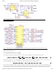
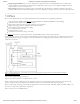
Figure 21. FPGA banks 0, 1 and 3. []
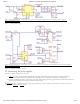
Figure 22 shows the voltage rails and decoupling for the FPGA.
The internal core of the FPGA is supplied 1.2V.
Banks 0 and 1 are supplied with the programmable VCCIO_PROG. By setting this from 1.2V to 3.3V, both inputs and IOs are set to be
compatible with the I/O standard LVCMOS of the respective voltage. Notice that a protected version of VCCIO_PROG is also available
to the user, as VCCIO_USR. This can be used to supply the Device/Circuit Under Test.
Bank 3 is supplied 1.5V, for compatibility with the DDR3 IC.
Bank 2 and VCCAUX are supplied 3.3V.