
Data Sheet

3/8/2018 Digital Discovery Reference Manual [Reference.Digilentinc]
https://reference.digilentinc.com/reference/instrumentation/digital-discovery/reference-manual 20/25
Programming the FPGA: There is no non-volatile FPGA configuration memory on the Digital Discovery. The WaveForms
software identifies the connected device and downloads an appropriate .bit file at power-up, via a Digilent USB-JTAG interface.
Adept run-time is used for low level protocols.
Data exchange: All instrument configuration data, acquired data and status information is handled via a Digilent synchronous
parallel bus and USB interface. Speed up to 20MB/sec. is reached, depending on USB port type and load as well as PC performance.
The core of the Digital Discovery is the Xilinx Spartan6 FPGA circuit XC6SLX25. The configured logic performs:
Clock management (12MHz and 60 MHz () for USB communication, 100MHz and 800MHz for data sampling)
Acquisition control and Data Storage (Logic Analyzer)
Digital signal synthesis (for pattern generator and bus protocol controllers)
Trigger system (trigger detection and distribution for all instruments)
Power supplies control and instruments enabling
Power and temperature monitoring
Calibration memory control
Communication with the PC (settings, status data)
Block RAM () of the FPGA is used for signal synthesis. External DDR3 memory is used for data acquisition.
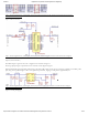
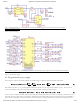
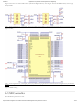
Detail of the trigger system is shown in Figure 20. Each instrument generates a trigger signal when a trigger condition is met. Each trigger
signal (including external triggers) can trigger any instrument and drive the external trigger outputs. This way, all the instruments can
synchronize to each other.
(https://reference.digilentinc.com/_detail/digital_discovery/dd_20fpgatriggerdiagram.png?id=reference%3Ainstrumentation%3Adigital-
discovery%3Areference-manual)
Figure 20. FPGA configuration trigger block diagram. []
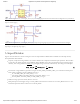
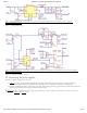
Figure 21 shows the connections to the FPGA banks 0, 1 and 3.
Bank 0 is used for IOs. DIO_FPGA pins are the actual input/output pins to be used with the Pattern Generator, Static IO and Logic
Analyzer. A DIO_PULL pin can add Pull-Up or Pull-Down resistors to the associated DIO_FPGA pin (see Figure 4).
Bank 1 is used for high speed Logic Analyzer inputs. DIN_FPGA are the actual input pins, while DIN_VREF_H and DIN_VREF_L set
the reference voltage for the input dividers (see Figure 9).
Bank 3 is used as port for the DDR3 memory.
7. FPGA