
Data Sheet

3/8/2018 Digital Discovery Reference Manual [Reference.Digilentinc]
https://reference.digilentinc.com/reference/instrumentation/digital-discovery/reference-manual 16/25
(https://reference.digilentinc.com/_detail/digital_discovery/dd_11vbusmonitoring.png?id=reference%3Ainstrumentation%3Adigital-
discovery%3Areference-manual)
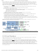
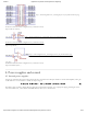
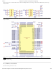
Figure 11 VBUS monitoring. []
.
(https://reference.digilentinc.com/_detail/digital_discovery/dd_12internalvoltagesupplies.png?id=reference%3Ainstrumentation%3Adigital-
discovery%3Areference-manual)
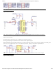
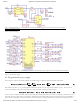
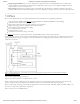
Figure 12. Internal voltage supplies. []
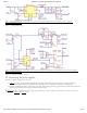
IC13 in Figure 13 generates the VCCIO_PROG, the variable voltage to supply the input and IO banks of the FPGA:
With VVSET_VCCIO ϵ (0…3V), VCCIO_PROG could be theoretically set in the range: VCCIO_PROG ϵ (1.02V…3.42V). IC15 is a
current shunt amplifier, with a gain of 100. With Vref = 0.75V and R115 = 50mΩ, the output voltage is:
IC14 is a window comparator: FAULT_USR is logical LOW, when VISNS_USR is either more than 1.5V (IVCCIO_USR>150mA) or less
than 0.66V (IVCCIO_USR←18mA). If this happens, the FPGA turns EN_PWR_USR to LOW, which turns both Q1A and Q1B OFF, to
protect VCCIO_USR against overcurrent and reverse current respectively. VCCIO_USR is halved to VSNS_USR, for being monitored.
4.2 Programmable power supply