
Data Sheet

3/8/2018 Digital Discovery Reference Manual [Reference.Digilentinc]
https://reference.digilentinc.com/reference/instrumentation/digital-discovery/reference-manual 14/25
(https://reference.digilentinc.com/_detail/digital_discovery/dd_6vu6v0supply.png?id=reference%3Ainstrumentation%3Adigital-discovery%3Areference-
manual)
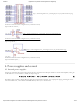
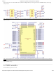
Figure 6. VU6V0 supply. []
(https://reference.digilentinc.com/_detail/digital_discovery/dd_7backpoweringvoltageclipper.png?id=reference%3Ainstrumentation%3Adigital-
discovery%3Areference-manual)
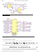
Figure Figure 7. Backpowering voltage clipper. []
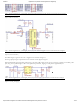
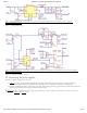
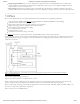
Figure 8 shows the DIN user connector and Figure 9 shows the Input Divider for DIN0. DIN1 to DIN23 use similar input circuitry.
The Input Dividers block includes:
Frequency compensated voltage dividers: 10/11 resistive dividers with compensation for FPGA input capacitance. All the dividers
together have the settable reference voltage VREFIO. Setting VREFIO close to the logical threshold voltage provides the highest
sensitivity, while setting VREFIO at GND () or logical supply voltage increase the noise immunity. The voltage at the FPGA pin:
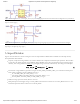
The reference voltage VREFIO is generated as in Figure 10. DIN_VREF_H and DIN_VREF_L are connected to FPGA pins in
bank 1. Bank1 is supplied at VCCIO. VREFIO can be set at:
0V, when DIN_VREF_H = DIN_VREF_L = low
0.43*VCCIO_PROG, when DIN_VREF_H = high, DIN_VREF_L = low
VCCIO_PROG, when DIN_VREF_H = DIN_VREF_L = high.
ESD/Overvoltage protection: Shottky diodes to VCC3V3.
DIN_FPGA pin: the bank supply voltage is VCCIO_PROG. The WaveForms software can set VCCIO_PROG from 1.2 to 3.3V.
The FPGA input threshold level is about 45% of VCCIO_PROG.
3. Input Dividers