
Data Sheet

3/8/2018 Digital Discovery Reference Manual [Reference.Digilentinc]
https://reference.digilentinc.com/reference/instrumentation/digital-discovery/reference-manual 12/25
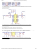
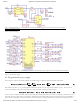
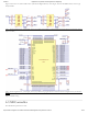
data into the DDR3 memory. Signals and equations also use certain naming conventions. Signals in the Input block use “DIN” prefix to
indicate these are inputs only. Signals in the Input/Output block use “DIO” prefix. Signals at the user connectors include “USR” in their
names, while signals at the FPGA pins include “FPGA”. Signals at the FPGA pins driving the pull resistors for DIO signals, include
“PULL” in their names. DIN inputs are indexed 0 to 23, DIO input/outputs are indexed 24 to 39. Memory signals have the “DDR” prefix.
Supply rails show the voltage with the VCC () prefix. Referring to the block diagram in Figure 2 below:
The I/O Level Translators build the bidirectional interface for input/output pins (used in the Pattern Generator, Static IO, and
Logic Analyzer)
The Input Dividers are the conditioning circuits for the input pins (used in the Logic Analyzer)
The FPGA banks are supplied at different voltages:
Bank 0, Bank1: VCCIO_PROG, a variable voltage, settable in the range 1.2V…3.3V. The logic standard is set to:
LVCMOS18_JEDEC. The threshold voltage is about 0.45*VCCIO_PROG.
Bank 2: VCC3V3, a fixed voltage of 3.3V.
Bank 3: VCC1V5, a fixed voltage of 1.5V.
A replica of VCCIO_PROG is also available to the user, as VCCIO_USR, under the V user switch control.
The DDR3 Data Memory block stores the Logic analyzer acquired data.
The Power Supplies and Control block generates all internal supply voltages as well as user supply programmable voltage. The
control block also monitors the device power consumption for USB compliance.
The USB Controller interfaces with the PC for programming the volatile FPGA memory after power on or when a new
configuration is requested. After that, it performs the data transfer between the PC and FPGA.
The Calibration Memory stores all calibration parameters. The Digital Discovery includes no analog calibration circuitry. Instead, a
calibration operation is performed at manufacturing (or by the user), and parameters are stored in memory. The WaveForms software
uses these parameters to adjust the acquired data and the generated signals.
In the sections that follow, schematics are not shown separately for identical blocks. For example, the Input Divider is only shown for
DIN0 since the schematic for all other DIN1…DIN23 is identical.
(https://reference.digilentinc.com/_detail/digital_discovery/dd_2blockdiagram.png?id=reference%3Ainstrumentation%3Adigital-discovery%3Areference-
manual)
Figure 2. Digital Discovery Hardware block diagram. []
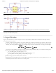
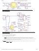
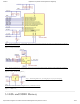
Figure 3 shows the DIO user connectors and Figure 4 shows the I/O level translator for DIO24. DIO25 to DIO31 use similar discrete
components, connected to pins 1A2…2A3, respectively 1B2…2B3 of IC2.
The I/O Level Translators block includes: - Input protection: series PTC (33Ω, positive thermal coefficient thermistor) and parallel
ESD/overvoltage diodes to 5.2V and GND (). - Voltage level translators, SN74CBT3384C. When DIO_USR signals are driven by the
DUT, the voltage at the FPGA pins is limited at VCCIO_SW-1V = 3.3V. When the FPGA drives DIO_USR signals, they pass unlimited
trough the low impedance SN74CBT3384C buffer. - Pull resistors: 10k, individually settable as Pull-Up, Pull-Down or High-Z. This is done
with a second FPGA pin associated to each DIO, which can be driven High, Low or HiZ. The Pull-Up voltage is VCCIO_PROG. -
DIO_FPGA pin: the bank supply voltage is VCCIO_PROG> The WaveForms software can set VCCIO_PROG from 1.2 to 3.3V. The
FPGA input threshold level is about 45% of VCCIO_PROG. The output strength can be set from 2mA to 16mA. The output slew rate can
be set as: Quiet, Slow or Fast.
2. I/O Level Translators