
Manual

Opus Card – DDR-2 Interface
Reference Manual
12/03/2010 07:35 AM 17
Copyright © 2009-2010 by CML
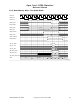
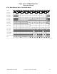
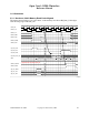
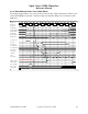
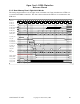
3.3.2 Non-burst, 32-bit Memory Read not Clock-Aligned
The timing diagram below is for a non-burst, 32-bit memory read where Rd_Data_Valid does
not align with the rising edge of Bus2IP_Clk.
1 2 3 4 5 6 7 8 9 10 11 12
Read
Address
Word1 Wo rd2
32-bit Data
Address
Idle Wait_RdValid IdleWai t_Rd Val i d Rd _Ack1 Rd_A ck2
Signals below are from write_ctrl
TimeGen
DDR2_Clk
Bus2IP_Clk
Bus2IP_CS
Bus2IP_RNW
Bus2IP_Addr
Bus2IP_RdReq
IP2Bus_Data
Rd_Send_Cmd
Rd_Send_Ack
Rd_Data_Valid
Rd_Data_FIFO_Out
State
IP2Bus_AddrAck
IP2Bus_RdAck
App_AF_WREn
App_AF_Cmd
App_AF_Addr