Opus Card – DDR-2 Interface Reference Manual Revision 0.02 0.03 0.04 0.10 1.00 Name Rick Hoover Rick Hoover – Added support for burst reads and writes Rick Hoover – Made corrections to Bus2IP_RdReq that match ChipScope traces. Basically Bus2IP_RdReq is active for only one clock on non-burst reads and is active one additional clock past the de-assertion of Bus2IP_CS for burst reads. Rick Hoover – Added support for burst of eight quadwords. This is required for DMA accesses.
Opus Card – DDR-2 Interface Reference Manual Table of Contents 1. INTRODUCTION ..................................................................................................................................................3 1.1 1.2 1.3 1.4 DEBUG REGISTERS ACCESSIBLE BY THE CPU .....................................................................................................3 CONFIGURATION REGISTER ACCESSIBLE BY THE CPU..................................................................................
Opus Card – DDR-2 Interface Reference Manual 1. Introduction This document provides the details on how DDR-2 memory on the Opus card is connected into the PLB bus contained in the Xilinx Virtex-5 FPGA using the Embedded Design Kit (EDK). The CML team discovered that the default Multi-Port Memory Controller (MPMC) provided with the EDK had problems which reduced the reliability of accessing the DDR-2 memory contained on the Opus card.
Opus Card – DDR-2 Interface Reference Manual 1.4 DDR-2 Memory Accessible by the CPU The DDR-2 memory is 128 MBytes in size, organized as 32-bit words. The memory is accessible from 0x88000000 to 0x8FFFFFFF. The C_CACHLINE_ADDR_MODE for the PLB interface in the DDR-2 memory controller MUST be set to 1 so that cache line bursts always start at the first address in the cache line. A setting of 0, which is the default, will not work with the current implementation of the DDR-2 memory controller.
Opus Card – DDR-2 Interface Reference Manual 2. State Machine for Writing Data to Memory This chapter covers the state machine that controls the writing of data sent via the PLB bus to the DDR-2 Memory Controller. The write state machine supports both non-burst writes and burst writes. Burst writes are limited to a multiple of four 32-bit words or a multiple of two 64-bit words depending on the width of the PLB data bus and should be limited to a maximum length of eight quad-words (128 bytes).
Opus Card – DDR-2 Interface Reference Manual 2.2 Write State Machine The write state machine currently has ten states to support the writing of data to memory. Transitions from one state to the next occur on the rising edge of DDR2_Clk and the state machine is synchronously reset to Idle when Bus2IP_Reset is ‘1’. Each state is described below: State Idle Description Waiting for a write from the PLB slave.
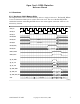
Opus Card – DDR-2 Interface Reference Manual 2.3 Waveforms 2.3.1 Non-burst, 32-bit Memory Write The diagram below is for a non-burst memory write to a single 32-bit word. The Bus2IP_BE bus is used to determine which bytes to write in the 32-bit word. The use of the Bus2IP_BE bus enables the hardware controlling the PLB slave to also write eight or sixteen bit values to a 32bit memory location.
Opus Card – DDR-2 Interface Reference Manual 2.3.2 Non-burst, 64-bit Memory Write The diagram below is for a non-burst memory write to a single 64-bit word. The Bus2IP_BE bus is used to determine which bytes to write in the 64-bit word. The use of the Bus2IP_BE bus enables the hardware controlling the PLB slave to also write eight, sixteen, or thirty-two bit values to a 64-bit memory location.
Opus Card – DDR-2 Interface Reference Manual 2.3.
Opus Card – DDR-2 Interface Reference Manual 2.3.
Opus Card – DDR-2 Interface Reference Manual 2.3.
Opus Card – DDR-2 Interface Reference Manual 2.3.
Opus Card – DDR-2 Interface Reference Manual 3. State Machines for Reading Data from Memory This chapter covers the state machines that controls the reading of data requested via the PLB bus from the DDR-2 Memory Controller. The read state machines support both non-burst reads and burst reads. Burst reads are limited to a multiple of four 32-bit words or a multiple of two 64-bit words depending on the width of the PLB data bus and should be limited to a maximum length of eight quad-words (128 bytes).
Opus Card – DDR-2 Interface Reference Manual 3.2 Read State Machine The read state machine currently has eight states to support the reading of data from memory via the DDR-2 memory controller. Transitions from one state to the next occur on the rising edge of DDR2_Clk and the state machine is synchronously reset to Idle when Bus2IP_Reset is ‘1’. Each state is described below: State Idle Description Waiting for a read request from the PLB slave.
Opus Card – DDR-2 Interface Reference Manual 3.2 Read FIFO State Machine The Read FIFO state machine currently has four states to support the reading of data from the read FIFO to the PLB slave. Transitions from one state to the next occur on the rising edge of DDR2_Clk and the state machine is synchronously reset to Idle when Bus2IP_Reset is ‘1’. Each state is described below: State Idle FIFO_Rd Hi_Bits Lo_Bits Description Waiting for the read FIFO to contain data during a burst read.
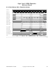
Opus Card – DDR-2 Interface Reference Manual 3.3 Waveforms 3.3.1 Non-burst, 32-bit Memory Read Clock-Aligned The timing diagram below is for a non-burst, 32-bit memory read where Rd_Data_Valid aligns with the rising edge of Bus2IP_Clk.
Opus Card – DDR-2 Interface Reference Manual 3.3.2 Non-burst, 32-bit Memory Read not Clock-Aligned The timing diagram below is for a non-burst, 32-bit memory read where Rd_Data_Valid does not align with the rising edge of Bus2IP_Clk.
Opus Card – DDR-2 Interface Reference Manual 3.3.3 Non-burst, 64-bit Memory Read The timing diagram below is for a non-burst, 64-bit memory read where Rd_Data_Valid aligns with the rising edge of Bus2IP_Clk. The non-aligned version of the read is similar except the Rd_Align state is skipped.
Opus Card – DDR-2 Interface Reference Manual 3.3.4 Burst Memory Read - Four 32-bit Words The timing diagram below is for a four 32-bit word burst read. Data is buffered to a FIFO as it is read from the DDR-2 controller. The data is then read from the FIFO as it is transferred to the PLB slave.
Opus Card – DDR-2 Interface Reference Manual 3.3.5 Burst Memory Read - Eight 32-bit Words The timing diagram below is for an eight 32-bit word burst read. Data is buffered to a FIFO as it is read from the DDR-2 controller. The data is then read from the FIFO as it is transferred to the PLB slave.
Opus Card – DDR-2 Interface Reference Manual 3.3.6 Burst Memory Read - Two 64-bit Words The timing diagram below is for a two 64-bit word burst read. Data is buffered to a FIFO as it is read from the DDR-2 controller. The data is then read from the FIFO as it is transferred to the PLB slave.
Opus Card – DDR-2 Interface Reference Manual 3.3.7 Burst Memory Read - Four 64-bit Words The timing diagram below is for a four 64-bit word burst read. Data is buffered to a FIFO as it is read from the DDR-2 controller. The data is then read from the FIFO as it is transferred to the PLB slave.