
Instruction Manual
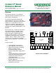


Cerebot II Reference Manual Digilent, Inc.
www.digilentinc.com page 9 of 10
Copyright Digilent, Inc. All rights reserved. Other product and company names mentioned may be trademarks of their respective owners.
Pin Description Cerebot II Pmod Header Pins to
ATmega64L Ports / Bit
JD SPI interface
The SPI interface on JD is used for synchronous serial
communication of host processor and peripherals or for a
connection of two processors. Master or slave modes are
selected as part of the software.
Serial port communications and interrupts
Asynchronous serial port, UART1, as well as the Atmel TWI
interface can be accessed on JD. These pins can also be
used as external interrupt sources.
Pin Function Port / Bit
1 SS PB 0
2 MOSI PB 2
3 MISO PB 3
4 SCK PB 1
5 GND
6 VCC
7 SCL/ INT0 PD 0
8 SDA/ INT1 PD 1
9 RXD1/ INT2 PD 2
10 TXD1/ INT3 PD 3
11 GND
12 VCC
JE H-bridge connection with input capture
This port can be used to provide two pulse width modulated
outputs to run two motors, or it can be used to run a single
motor with input sensing for a shaft encoder or other sensor.
The PmodHB3 or PmodHB5 can be used for this application.
1 T1 PD 6
2 OC1A PB 5
3 ICP1 PD 4
4 OC1B PB 6
5 GND
6 VCC
JF H-bridge connection, interrupts, and on-board LEDs
Use this port to run two motors, like JE, or a motor with input
sensing for a shaft encoder or other sensor. All of the pins on
this header give access to interrupt inputs, providing flexibility
for application development. JF can be used as a motor
controller or interrupt source. The onboard LEDs share pins
with this header and can display information.
1 T3/ INT6 PE 6
2 OC3B/ INT4 PE 4
3 ICP3/ INT7 PE 7
4 OC3C/ INT5 PE 5
5 GND
6 VCC
JG H-bridge connection
This port can be used to provide two pulse width modulated
outputs to run two motors, or it can be used to run a single
motor with input sensing for a shaft encoder or other sensor.
The PmodHB3 or PmodHB5 can be used for this application.
1 T2 PD 7
2 OC0 PB 4
3 XCK1 PD 5
4 OC2/ OC1C PB 7
5 GND
6 VCC
JH Analog input
Inputs to the analog to digital converter of the ATmega64L.
ADC0 and ADC1 are connected to the Cerebot II’s voltage
monitoring circuits. ADC0 is the input for monitoring VU board
power and ADC1 is connected to VS for monitoring the
independent servo power.
The default fuse setting for the Cerebot II is to disable the
JTAG input and provide analog inputs. The ATmega64L fuse
settings have to be changed to enable the JTAG interface to
use JH as a JTAG device input (e.g., to use the Atmel
JTAGICE mkII).
The pins on JH are shared with the servo connectors S1-S8.
1 ADC0 PF 0
2 ADC1 PF 1
3 ADC2 PF 2
4 ADC3 PF 3
5 GND
6 VCC
7 ADC5/ TMS PF 5
8 ADC7/ TDI PF 7
9 ADC6/ TDO PF 6
10 ADC4/ TCK PF 4
11 GND
12 VCC