
Data Sheet

3/8/2018 Arty Z7 Reference Manual [Reference.Digilentinc]
https://reference.digilentinc.com/reference/programmable-logic/arty-z7/reference-manual 9/24
Unlike Xilinx FPGA devices, APSoC devices such as the Zynq-7020 are designed around the processor, which acts as a master to the
programmable logic fabric and all other on-chip peripherals in the processing system. This causes the Zynq boot process to be more similar
to that of a microcontroller than an FPGA. This process involves the processor loading and executing a Zynq Boot Image, which includes a
First Stage Bootloader (FSBL), a bitstream for configuring the programmable logic (optional), and a user application. The boot process is
broken into three stages:
Stage 0
After the Arty Z7 is powered on or the Zynq is reset (in software or by pressing SRST), one of the processors (CPU0) begins executing an
internal piece of read-only code called the BootROM. If and only if the Zynq was just powered on, the BootROM will first latch the state of
the mode pins into the mode register (the mode pins are attached to JP4 on the Arty Z7). If the BootROM is being executed due to a reset
event, then the mode pins are not latched, and the previous state of the mode register is used. This means that the Arty Z7 needs a power
cycle to register any change in the programming mode jumper (JP4). Next, the BootROM copies an FSBL from the form of non-volatile
memory specified by the mode register to the 256 KB of internal RAM () within the APU (called On-Chip Memory, or OCM). The FSBL
must be wrapped up in a Zynq Boot Image in order for the BootROM to properly copy it. The last thing the BootROM does is hand off
execution to the FSBL in OCM.
Stage 1
During this stage, the FSBL first finishes configuring the PS components, such as the DDR memory controller. Then, if a bitstream is
present in the Zynq Boot Image, it is read and used to configure the PL. Finally, the user application is loaded into memory from the Zynq
Boot Image, and execution is handed off to it.
Stage 2
The last stage is the execution of the user application that was loaded by the FSBL. This can be any sort of program, from a simple “Hello
World” design, to a Second Stage Boot loader used to boot an operating system like Linux. For a more thorough explanation of the boot
process, refer to Chapter 6 of the Zynq Technical Reference manual (http://www.xilinx.com/support/documentation/user_guides/ug585-
Zynq-7000-TRM.pdf).
The Zynq Boot Image is created using Vivado and Xilinx Software Development Kit (Xilinx SDK). For information on creating this image
please refer to the available Xilinx documentation for these tools.
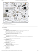
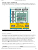
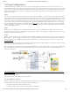
The Arty Z7 supports three different boot modes: microSD, Quad SPI Flash, and JTAG. The boot mode is selected using the Mode jumper
(JP4), which affects the state of the Zynq configuration pins after power-on. Figure 3.1 depicts how the Zynq configuration pins are
connected on the Arty Z7.
(https://reference.digilentinc.com/_detail/reference/programmable-logic/arty-z7/arty-z7-config.png?id=reference%3Aprogrammable-logic%3Aarty-
z7%3Areference-manual)
Figure 3.1. Arty Z7 configuration pins.
The three boot modes are described in the following sections.
The Arty Z7 supports booting from a microSD card inserted into connector J9. The following procedure will allow you to boot the Zynq
from microSD with a standard Zynq Boot Image created with the Xilinx tools:
1. Format the microSD card with a FAT32 file system.
2. Copy the Zynq Boot Image created with Xilinx SDK to the microSD card.
3 Zynq Configuration
3.1 microSD Boot Mode