
Data Sheet

3/8/2018 Arty Z7 Reference Manual [Reference.Digilentinc]
https://reference.digilentinc.com/reference/programmable-logic/arty-z7/reference-manual 6/24
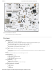
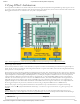
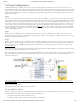
The Zynq APSoC is divided into two distinct subsystems: The Processing System (PS) and the Programmable Logic (PL). Figure 2.1 shows
an overview of the Zynq APSoC architecture, with the PS colored light green and the PL in yellow. Note that the PCIe Gen2 controller and
Multi-gigabit transceivers are not available on the Zynq-7020 or Zynq-7010 devices.
(https://reference.digilentinc.com/_detail/zybo/zyng1.png?id=reference%3Aprogrammable-logic%3Aarty-z7%3Areference-manual)
Figure 2.1 Zynq APSoC architecture
The PL is nearly identical to a Xilinx 7-series Artix FPGA, except that it contains several dedicated ports and buses that tightly couple it to
the PS. The PL also does not contain the same configuration hardware as a typical 7-series FPGA, and it must be configured either directly
by the processor or via the JTAG port.
The PS consists of many components, including the Application Processing Unit (APU, which includes 2 Cortex-A9 processors), Advanced
Microcontroller Bus Architecture (AMBA) Interconnect, DDR3 Memory controller, and various peripheral controllers with their inputs and
outputs multiplexed to 54 dedicated pins (called Multiplexed I/O, or MIO pins). Peripheral controllers that do not have their inputs and
outputs connected to MIO pins can instead route their I/O through the PL, via the Extended-MIO (EMIO) interface. The peripheral
controllers are connected to the processors as slaves via the AMBA interconnect, and contain readable/writable control registers that are
addressable in the processors’ memory space. The programmable logic is also connected to the interconnect as a slave, and designs can
implement multiple cores in the FPGA fabric that each also contain addressable control registers. Furthermore, cores implemented in the
PL can trigger interrupts to the processors (connections not shown in Fig. 3) and perform DMA accesses to DDR3 memory.
There are many aspects of the Zynq APSoC architecture that are beyond the scope of this document. For a complete and thorough
description, refer to the Zynq Technical Reference manual (http://www.xilinx.com/support/documentation/user_guides/ug585-Zynq-7000-
TRM.pdf).
Table 2.1 depicts the external components connected to the MIO pins of the Arty Z7. The Zynq Presets File found on the Arty Z7
Resource Center (https://reference.digilentinc.com/reference/programmable-logic/arty-z7/start) can be imported into EDK and Vivado Designs
to properly configure the PS to work with these peripherals.
MIO 500 3.3 V Peripherals
2 Zynq APSoC Architecture