
Data Sheet

3/8/2018 Arty Z7 Reference Manual [Reference.Digilentinc]
https://reference.digilentinc.com/reference/programmable-logic/arty-z7/reference-manual 14/24
The RGMII specification calls for the receive (RXC) and transmit clock (TXC) to be delayed relative to the data signals (RXD[0:3], RXCTL
and TXD[0:3], TXCTL). Xilinx PCB guidelines also require this delay to be added. The RTL8211E-VL is capable of inserting a 2ns delay on
both the TXC and RXC so that board traces do not need to be made longer.
The PHY is clocked from the same 50 MHz () oscillator that clocks the Zynq PS. The parasitic capacitance of the two loads is low enough
to be driven from a single source.
On an Ethernet network each node needs a unique MAC address. To this end, the one-time-programmable (OTP) region of the Quad-SPI
flash has been programmed at the factory with a 48-bit globally unique EUI-48/64™ compatible identifier. The OTP address range
[0x20;0x25] contains the identifier with the first byte in transmission byte order being at the lowest address. Refer to the Flash memory
datasheet (http://www.cypress.com/file/177966/download) for information on how to access the OTP regions. When using Petalinux, this is
automatically handled in the U-boot boot-loader, and the Linux system is automatically configured to use this unique MAC address.
For more information on using the Gigabit Ethernet MAC, refer to the Zynq Technical Reference manual
(http://www.xilinx.com/support/documentation/user_guides/ug585-Zynq-7000-TRM.pdf).
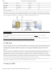
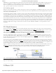
The Arty Z7 contains two unbuffered HDMI ports: one source port J11 (output), and one sink port J10 (input). Both ports use HDMI type-
A receptacles with the data and clock signals terminated and connected directly to the Zynq PL.
Both HDMI and DVI systems use the same TMDS signaling standard, directly supported by Zynq PL's user I/O infrastructure. Also,
HDMI sources are backward compatible with DVI sinks, and vice versa. Thus, simple passive adaptors (available at most electronics stores)
can be used to drive a DVI monitor or accept a DVI input. The HDMI receptacle only includes digital signals, so only DVI-D mode is
possible.
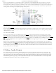
The 19-pin HDMI connectors include three differential data channels, one differential clock channel five GND () connections, a one-wire
Consumer Electronics Control (CEC) bus, a two-wire Display Data Channel (DDC) bus that is essentially an I2C bus, a Hot Plug Detect
(HPD) signal, a 5V signal capable of delivering up to 50mA, and one reserved (RES) pin. All non-power signals are wired to the Zynq PL
with the exception of RES.
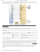
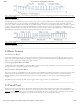
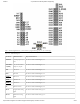
Pin/Signal J11 (source) J10 (sink)
Description FPGA
pin
Description FPGA
pin
D[2]_P,
D[2]_N
Data output J18, H18 Data input N20,
P20
D[1]_P,
D[1]_N
Data output K19, J19 Data input T20,
U20
D[0]_P,
D[0]_N
Data output K17,
K18
Data input V20,
W20
CLK_P,
CLK_N
Clock output L16,
L17
Clock input N18,
P19
CEC Consumer Electronics Control bidirectional
(optional)
G15 Consumer Electronics Control bidirectional
(optional)
H17
SCL, SDA DDC bidirectional (optional) M17,
M18
DDC bidirectional U14,
U15
HPD/HPA Hot-plug detect input (inverted, optional) R19 Hot-plug assert output T19
Table 10.1. HDMI pin description and assignment.
10 HDMI
10.1 TMDS Signals