
Data Sheet

3/8/2018 Arty Z7 Reference Manual [Reference.Digilentinc]
https://reference.digilentinc.com/reference/programmable-logic/arty-z7/reference-manual 11/24
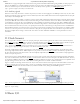
Both the memory chips and the PS DDR bank are powered from the 1.5V supply. The mid-point reference of 0.75V is created with a
simple resistor divider and is available to the Zynq as external reference.
For proper operation it is essential that the PS memory controller is configured properly. Settings range from the actual memory flavor to
the board trace delays. For your convenience, the Zynq presets file for the Arty Z7 is provided on the resource center
(https://reference.digilentinc.com/reference/programmable-logic/arty-z7/start) and automatically configures the Zynq Processing System IP core
with the correct parameters.
For best DDR3 performance, DRAM training is enabled for write leveling, read gate, and read data eye options in the PS Configuration
Tool in Xilinx tools. Training is done dynamically by the controller to account for board delays, process variations and thermal drift.
Optimum starting values for the training process are the board delays (propagation delays) for certain memory signals.
Board delays are specified for each of the byte groups. These parameters are board-specific and were calculated from the PCB trace length
reports. The DQS to CLK Delay and Board Delay values are calculated specific to the Arty Z7 memory interface PCB design.
For more details on memory controller operation, refer to the Xilinx Zynq Technical Reference manual
(http://www.xilinx.com/support/documentation/user_guides/ug585-Zynq-7000-TRM.pdf).
¹Maximum actual clock frequency is 525 MHz () on the Arty Z7 due to PLL limitation.
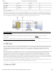
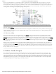
The Arty Z7 includes an FTDI FT2232HQ USB-UART bridge (attached to connector J14) that lets you use PC applications to
communicate with the board using standard COM port commands (or the tty interface in Linux). Drivers are automatically installed in
Windows and newer versions of Linux. Serial port data is exchanged with the Zynq using a two-wire serial port (TXD/RXD). After the
drivers are installed, I/O commands can be used from the PC directed to the COM port to produce serial data traffic on the Zynq pins. The
port is tied to PS (MIO) pins and can be used in combination with the UART 0 controller.
The Zynq presets file (available in the Arty Z7 Resource Center (https://reference.digilentinc.com/reference/programmable-logic/arty-z7/start))
takes care of mapping the correct MIO pins to the UART 0 controller and uses the following default protocol parameters: 115200 baud rate,
1 stop bit, no parity, 8-bit character length.
Two on-board status LEDs provide visual feedback on traffic flowing through the port: the transmit LED () (LD11) and the receive LED ()
(LD10). Signal names that imply direction are from the point-of-view of the DTE (Data Terminal Equipment), in this case the PC.
The FT2232HQ is also used as the controller for the Digilent USB-JTAG circuitry, but the USB-UART and USB-JTAG functions behave
entirely independent of one another. Programmers interested in using the UART functionality of the FT2232 within their design do not
need to worry about the JTAG circuitry interfering with the UART data transfers, and vice-versa. The combination of these two features
into a single device allows the Arty Z7 to be programmed, communicated with via UART, and powered from a computer attached with a
single Micro USB cable.
The DTR signal from the UART controller on the FT2232HQ is connected to MIO12 of the Zynq device via JP1. Should the Arduino IDE
be ported to work with the Arty Z7, this jumper can be shorted and MIO12 could be used to place the Arty Z7 in a “ready to receive a new
sketch” state. This would mimic the behavior of typical Arduino IDE boot-loaders.
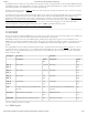
The Arty Z7 provides a microSD slot (J9) for non-volatile external memory storage as well as booting the Zynq. The slot is wired to Bank
1/501 MIO[40-47], including Card Detect. On the PS side peripheral SDIO 0 is mapped out to these pins and controls communication with
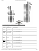
the SD card. The pinout can be seen in Table 7.1. The peripheral controller supports 1-bit and 4-bit SD transfer modes, but does not
support SPI mode. Based on the Zynq Technical Reference manual (http://www.xilinx.com/support/documentation/user_guides/ug585-Zynq-
7000-TRM.pdf), SDIO host mode is the only mode supported.
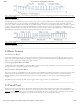
Signal Name Description Zynq Pin SD Slot Pin
SD_D0 Data[0] MIO42 7
SD_D1 Data[1] MIO43 8
SD_D2 Data[2] MIO44 1
SD_D3 Data[3] MIO45 2
6 USB UART Bridge (Serial Port)
7 microSD Slot