
Data Sheet

3/8/2018 Arty Z7 Reference Manual [Reference.Digilentinc]
https://reference.digilentinc.com/reference/programmable-logic/arty-z7/reference-manual 10/24
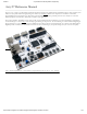
3. Rename the Zynq Boot Image on the microSD card to BOOT.bin.
4. Eject the microSD card from your computer and insert it into connector J9 on the Arty Z7.
5. Attach a power source to the Arty Z7 and select it using JP5.
6. Place a single jumper on JP4, shorting the two top pins (labeled “SD”).
7. Turn the board on. The board will now boot the image on the microSD card.
The Arty Z7 has an onboard 16MB Quad-SPI Flash that the Zynq can boot from. Documentation available from Xilinx describes how to
use Xilinx SDK to program a Zynq Boot Image into a Flash device attached to the Zynq. Once the Quad SPI Flash has been loaded with a
Zynq Boot Image, the following steps can be followed to boot from it:
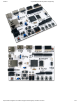
1. Attach a power source to the Arty Z7 and select it using JP5.
2. Place a single jumper on JP4, shorting the two center pins (labeled “QSPI”).
3. Turn the board on. The board will now boot the image stored in the Quad SPI flash.
When placed in JTAG boot mode, the processor will wait until software is loaded by a host computer using the Xilinx tools. After software
has been loaded, it is possible to either let the software begin executing, or step through it line by line using Xilinx SDK.
It is also possible to directly configure the PL over JTAG, independent of the processor. This can be done using the Vivado Hardware
Server.
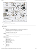
The Arty Z7 is configured to boot in Cascaded JTAG mode, which allows the PS to be accessed via the same JTAG port as the PL. It is also
possible to boot the Arty Z7 in Independent JTAG mode by loading a jumper in JP2 and shorting it. This will cause the PS to not be
accessible from the onboard JTAG circuitry, and only the PL will be visible in the scan chain. To access the PS over JTAG while in
independent JTAG mode, users will have to route the signals for the PJTAG peripheral over EMIO, and use an external device to
communicate with it.
The Arty Z7 features a Quad SPI serial NOR flash. The Spansion S25FL128S is used on this board. The Multi-I/O SPI Flash memory is
used to provide non-volatile code and data storage. It can be used to initialize the PS subsystem as well as configure the PL subsystem.
The relevant device attributes are:
16 MB ()
x1, x2, and x4 support
Bus speeds up to 104 MHz (), supporting Zynq configuration rates @ 100 MHz (). In Quad SPI mode, this translates to 400Mbs
Powered from 3.3V
The SPI Flash connects to the Zynq-7000 APSoC and supports the Quad SPI interface. This requires connection to specific pins in MIO
Bank 0/500, specifically MIO[1:6,8] as outlined in the Zynq datasheet. Quad-SPI feedback mode is used, thus qspi_sclk_fb_out/MIO[8] is
left to freely toggle and is connected only to a 20K pull-up resistor to 3.3V. This allows a Quad SPI clock frequency greater than
FQSPICLK2 (See the Zynq Technical Reference manual (http://www.xilinx.com/support/documentation/user_guides/ug585-Zynq-7000-
TRM.pdf) for more on this).
The Arty Z7 includes an IS43TR16256A-125KBL DDR3 memory components creating a single rank, 16-bit wide interface and a total of
512MiB of capacity. The DDR3 is connected to the hard memory controller in the Processor Subsystem (PS), as outlined in the Zynq
documentation.
The PS incorporates an AXI memory port interface, a DDR controller, the associated PHY, and a dedicated I/O bank. DDR3 memory
interface speeds up to 533 MHz ()/1066 Mbps are supported¹.
Arty Z7 was routed with 40 ohm (+/-10%) trace impedance for single-ended signals, and differential clock and strobes set to 80 ohms
(+/-10%). A feature called DCI (Digitally Controlled Impedance) is used to match the drive strength and termination impedance of the PS
pins to the trace impedance. On the memory side, each chip calibrates its on-die termination and drive strength using a 240 ohm resistor on
the ZQ pin.
Due to layout reasons, the two data byte groups (DQ[0-7], DQ[8-15]) were swapped. To the same effect, the data bits inside byte groups
were swapped as well. These changes are transparent to the user. During the whole design process the Xilinx PCB guidelines were followed.
3.2 Quad SPI Boot Mode
3.3 JTAG Boot Mode
4 Quad SPI Flash
5 DDR Memory