
MCC USB-1808X: High-Speed, High-Precision, Simultaneous USB DAQ Device - Datasheet
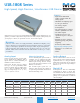
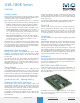
Table Of Contents

Measurement Computing (508) 946-5100
4
info@mccdaq.com mccdaq.com
USB-1808 Series
Specifications
These specifications apply to both standard and OEM versions unless noted.
All specifications are subject to change without notice.
Typical for 25 °C unless otherwise specified.
Analog Input
A/D converter type: Simultaneous
ADC resolution: 18 bits
Number of channels: 8 differential (DIFF), 8 single-ended (SE); software-selectable
per-channel for SE or DIFF
Input voltage range: ±10 V, ±5 V, 0 V to 10 V, 0 V to 5 V; software-selectable
per channel
Absolute max input voltage (CHx relative to AGND): ±25 V max (power on);
±15 V max (power off)
Input impedance: >1 GΩ (power on); 1000 Ω (power off)
Input bias current: ±50 pA
Input bandwidth, all input ranges, small signal (–3 dB): 2.0 MHz
Input capacitance: 50 pf
Specifications
Common mode voltage range
±10 V range: ±10.1 V
±5 V range: ±10.1 V
0 V to 10 V range: ±10.1 V
0 V to 5 V range: ±10.1 V
Common mode rejection ratio (f
IN
≤ 1 kHz, all input ranges): 90 dB
Crosstalk (±10 V, adjacent channels, DC to 100 kHz): –95 dB
Input coupling: DC
Sample rate
USB-1808: 0.023 Hz to 50 kHz; software-selectable
USB-1808X: 0.023 Hz to 200 kHz; software-selectable
Scan clock source: Internal input scan clock or external input scan clock (ICLKI pin)
Trigger source
ITRIG (see External Trigger on page 6)
Digital pattern detection (see Pattern Trigger on page 6)
Channel gain queue (up to 8 elements): Software-selectable. Queue list may
contain up to eight elements of unique, consecutive channels paired with
any valid range.
Warm-up time: 15 minutes min
FP
GA
FPGA
DI
O
Pr
otect
i
on
DIO
Protection
4
Mi
c
r
oco
n
t
r
o
ll
e
r wi
th
U
SB 2.0 High-Spee
d
I
nter
f
ac
e
Microcontroller with
USB 2.0 High-Speed
Interface
US
B
P
ort
USB
Port
Power Supp
l
ie
s
with Shutdown
an
d
So
f
t Star
t
Power Supplies
with Shutdown
and Soft Start
Bi
t
wi
se
Programmabl
e
D
I
O
Bitwise
Programmable
DIO
x8
8
Analog Input
EEPROM
EEPROM
24 MHz
M
C
r
y
sta
l
y
24 MHz
Crystal
Signal I/O Connector
Signal I/O Connector
18-bit
18 bit
ADC
18-bit
ADC
Buer
Buer
Buer
x2
2
Analog Output
16-bit
16 bit
D
AC
16-bit
DAC
Buer
Counter Input
2
Timer Output
2
Quad Counter Input
2
Clock Output
2
Clock Input
2
Trigger Input
2
Analog Input DC Voltage Measurement Accuracy (All Values are (±))
Range Gain Error
(% of Reading)
Offset Error
(mV)
INL Error
(% of range)
Absolute Accuracy
at Full Scale
(mV)
Gain Temperature
Coefficient
(% reading/°C)
Offset Temperature
Coefficient
(µV/°C)
±10 V 0.020 1.5 0.00076 3.576 0.00023 4
±5 V 0.020 1.0 0.00057 2.028 0.00023 4
0 V to 10 V 0.020 1.5 0.00028 3.528 0.00023 4
0 V to 5 V 0.020 1.0 0.00014 2.007 0.00023 4
Dynamic Performance
±10 V range
Signal-to-noise ratio (SNR): 94 dB
Signal-to-noise-and-distortion ratio (SINAD): 94 dB
Total harmonic distortion (THD): –108 dB
Spurious free dynamic range (SFDR): 112 dB
Effective number of bits (ENOB): 15.3 bits
±5 V range
SNR: 91 dB
SINAD: 91 dB
THD: –105 dB
SFDR: 107 dB
ENOB: 14.8 bits
0 V to 10 V range
SNR: 87 dB
SINAD: 87 dB
THD: –104 dB
SFDR: 109 dB
ENOB: 14.5 bits
0 V to 5 V range
SNR: 83 dB
SINAD: 83 dB
THD: –103 dB
SFDR: 103 dB
ENOB: 13.6 bits