
MCC USB-1608G Series High-Speed Multifunction USB DAQ (USB-1608GX) - Datasheet
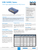
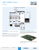
Table Of Contents

Measurement Computing (508) 946-5100
4
info@mccdaq.com mccdaq.com
USB-1608G Series
Noise Performance*
Range Counts LSBrms
±10 V 6 0.91
±5 V 6 0.91
±2 V 7 1.06
±1 V 9 1.36
* For the peak-to-peak noise distribution test, a differential input channel is con-
nected to AGND at the input terminal block, and 32,000 samples are acquired at
the maximum rate available at each setting.
Settling Time**
USB-1608G
Range 4 µS settling
accuracy
(% FSR)
6 µS settling
accuracy
(% FSR)
10 µS set-
tling accu-
racy
(% FSR)
±10 V 0.0061 0.0031 0.0015
±5 V 0.0061 0.0031 0.0015
±2 V 0.0061 0.0031 0.0015
±1 V
0.0061
0.0031 0.0015
USB-1608GX/1608GX-2AO
Range 2 µS settling
accuracy
(% FSR)
4 µS settling
accuracy
(% FSR)
9 µS settling
accuracy
(% FSR)
±10 V
0.1251
0.0031 0.0015
±5 V
0.0687
0.0031 0.0015
±2 V 0.0687 0.0031 0.0015
±1 V 0.0687 0.0031 0.0015
Specifications
** Settling time is defined as the expected accuracy after one conversion when
switching from a channel with a DC input at one extreme of full scale to another
channel with a DC input at the other extreme of full scale. Both input channels
are configured for the same input range.
Analog Output (USB-1608GX-2AO only)
Number of channels: 2 (leave unused AOUTx output channels disconnected)
Resolution: 16 bits
Output range: ±10 V (calibrated)
Output transient
Host computer is reset, powered on, suspended, or a reset command is
issued to the device
Duration: 500 µs
Amplitude: 2 V pk-pk
Powered off
Duration: 10 ms
Amplitude: 7 V peak
Differential non-linearity: ±0.25 LSB typ; ±1 LSB max
Output current
AOUTx: ±3.5 mA max
Output short-circuit protection
AOUTx connected to AGND: Unlimited duration
Output coupling: DC
Power on and reset state
DACs cleared to zero-scale: 0 V, ±50 mV (AOUTx defaults to 0 V when the host
is reset, powered on, suspended, or a reset command is issued to the device)
Output noise: 30 µVrms
Trigger source: TRIG (refer to “External Trigger” on page 5)
Sample clock source: Internal D/A clock or external D/A clock (AOCKI terminal)
Output update rate: 500 kHz/number of channels in the scan
Settling Time
To rated accuracy, 10 V step: 40 µs
Slew rate: 9 V/µs
Throughput
Software paced: 33 S/s to 4000 S/s typ, system-dependent
Hardware paced: 500 kS/s max, system-dependent
Specifications
These specifications apply to both standard and OEM versions unless noted.
Analog Input
A/D converter type: Successive approximation
ADC resolution: 16 bits
Number of channels: 8 DIFF, 16 SE; software-selectable
Input voltage range: ±10 V, ±5 V, ±2 V, ±1 V; software-selectable per channel
Absolute maximum input voltage
CHx relative to AGND: ±25 V max (power on); ±15 V max (power off)
Input Impedance: 1 GΩ (power on); 820 Ω (power off)
Input bias current: ±10 nA
Input bandwidth, all input ranges, small signal (–3 dB)
USB-1608G: 750 kHz
USB-1608GX/1608GX-2AO: 870 kHz
Input capacitance: 60 pf
Maximum working voltage (signal + common mode)
±10 V range: ±10.2 V max relative to AGND
±5 V range: ±10.2 V max relative to AGND
±2 V range: ±9.5 V max relative to AGND
±1 V range: ±9.0 V max relative to AGND
Common mode rejection ratio
f
IN
= 60 Hz, all input ranges: 86 dB
Crosstalk
Adjacent differential mode channels, DC to 100 kHz: –75 dB
Input coupling: DC
Sampling rate (software-selectable)
USB-1608G: 0.0149 Hz to 250 kHz
USB-1608GX/1608GX-2AO: 0.0149 Hz to 500 kHz
Trigger source: TRIG (refer to “External Trigger” on page 5)
Sample clock source: Internal A/D clock or external A/D clock (AICKI terminal)
Burst mode: Software-selectable using the internal A/D clock; always enabled
when using the external clock (AICKI terminal)
USB-1608G: 4 µs
USB-1608GX/1608GX-2AO: 2 µs
Throughput
Software paced: 33 to 4000 S/s typ, system dependent
Hardware paced
USB-1608G: 250 kS/s max
USB-1608GX/1608GX-2AO: 500 kS/s max
Channel gain queue: Up to 16 elements; software-selectable range for each channel
Warm-up time:15 minutes min
Analog Input DC Voltage Measurement
All Values are (±)
Range Gain Error
(% of Reading)
Offset Error
(µV)
INL Error
(% of Range)
Absolute Accuracy
at Full Scale
(µV)
Gain Temperature
Coefficient
(% reading/°C)
Offset Temperature
Coefficient
(µV/°C)
±10 V 0.024 915 0.0076 4075 0.0014 47
±5 V 0.024 686 0.0076 2266 0.0014 24
±2 V 0.024 336 0.0076 968 0.0014 10
±1 V 0.024 245 0.0076 561 0.0014 5