
MCC USB-200 Series Single Gain Multifunction USB DAQ Devices (USB-202) - Datasheet
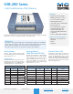
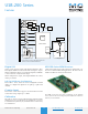
Table Of Contents

Measurement Computing (508) 946-5100
4
info@mccdaq.com mccdaq.com
USB-200 Series
Specifications
Specifications
All specifications are subject to change without notice.
Typical for 25 ˚C unless otherwise specified.
These specifications apply to both standard and OEM versions unless otherwise
specified.
Analog Input
A/D converter type: Successive approximation
ADC resolution: 12 bits
Number of channels: 8 SE
Input voltage range: ±10 V max
Absolute maximum input voltage
CHx to GND: ±25 V max (power on or power off)
Input impedance: 1 MΩ (power on or power off)
Input bias current
10 V input: –12 µA
0 V input: 2 µA
–10 V input: 12 µA
Input bandwidth, small signal (–3 dB)
USB-201/202: 150 kHz
USB-204/205: 1.0 MHz
Maximum working voltage
Input range relative to AGND: ±10.1 V max
Crosstalk (adjacent channels, DC to 10 kHz): –75 dB
Input coupling: DC
Sample rate
Internal pacer
USB-201/202: 0.016 S/s to 100 kS/s, software-selectable
USB-204/205: 0.016 S/s to 500 kS/s, software-selectable
External pacer
USB-201/202: 100 kS/s max
USB-204/205: 500 kS/s max
Sample clock source
Internal A/D clock
Pacer input terminal AICKI
Channel queue: Up to eight unique, ascending channels
Throughput
Software paced: 33 S/s to 4000 S/s typ, system dependent
Hardware paced
USB-201/202: 100 kS/s max, system dependent
USB-204/205: 500 kS/s max, system dependent
Warm-up time: 15 minutes min
Accuracy
Analog Input DC Voltage Measurement Accuracy
Range: ±10 V
Gain error (% of reading): 0.098
Offset error: 11 mV
Absolute accuracy at full scale: 20.8 mV
Gain temperature coefficient(% reading/°C): 0.016
Offset temperature coefficient (mV/°C): 0.87
Noise Performance
For peak to peak noise distribution, the input channel is connected to AGND at the
input terminal block, and 12,000 samples are acquired at the maximum throughput.
Range: ±10 V
Counts: 5
LSBrms: 0.76
Analog Input Calibration
Recommended warm-up time: 15 minutes min
Calibration method: Factory
Calibration interval: 1 year
Analog Output (USB-202, USB-205 only)
Resolution: 12 bits, 1 in 4,096
Output range: 0 V to 5.0 V
Number of channels: 2
Throughput, software paced: 250 S/s single channel typ, PC dependent
Maximum throughput when scanning is machine dependent.
Power on and reset voltage, initializes to 000h code: 0 V, ±10 mV
Output drive, each D/A OUT: 5 mA, sourcing
Slew rate: 0.8 V/µs typ
Analog Output Accuracy
All values are (±); accuracy tested at no load.
Range: 0 V to 5.0 V
Accuracy (LSB): 5.0 typ, 45.0 max
Analog Output Accuracy Components
All values are (±)
Range: 0 V to 5.0 V
% of FSR: 0.08 typ, 0.72 max
Gain error at FS (mV): 4.0 typ, 36.0 max
Offset (mV): 1.0 typ, 9.0 max
Zero-scale offsets may result in a fixed zero-scale error producing a “dead-band”
digital input code region. Changes in digital input code at values less than
0x040 may not produce a corresponding change in the output voltage. The
offset error is tested and specified at code 0x040.
Accuracy at FS (mV): 5.0 typ, 45.0 max
Digital I/O
Digital type: TTL
Number of I/O: 8
Configuration: Each bit may be configured as input (power on default) or output
Pull-up configuration: The port has 47 kΩ resistors that may be configured as pull-
up or pull-down with an internal jumper. The factory configuration is pull-down.
Digital I/O transfer rate (system-paced): 33 to 4000 port reads/writes per second
typical, system dependent
Input low voltage threshold: 0.8 V max
Input high voltage threshold: 2.0 V min
Input voltage limits: 5.5 V absolute max, –0.5 V absolute min, 0 V recommended
min
Output high voltage: 4.4 V min (IOH = –50 µA), 3.76 V min (IOH = –24 mA)
Output low voltage: 0.1 V max (IOL = 50 µA), 0.44 V max (IOL = 24 mA)
Output current: ±24 mA max
External Digital Trigger
Trigger source: TRIG input
Trigger mode: Software-selectable for edge or level sensitive, rising or falling edge,
high or low level. Power on default is edge sensitive, rising edge.
Trigger latency: 1 µs + 1 pacer clock cycle max
Trigger pulse width: 125 ns min
Input type: Schmitt trigger, 47 kΩ pull-down to ground
Schmitt trigger hysteresis: 1.01 V typ, 0.6 V min, 1.5 V max
Input high voltage threshold: 2.43 V typ, 1.9 V min, 3.1 V max
Input low voltage threshold: 1.42 V typ, 1.0 V min, 2.0 V max
Input voltage limits: 5.5 V absolute max, –0.5 V absolute min, 0 V recommended
min
External Pacer Input/Output
Terminal names: AICKI, AICKO
Terminal types
AICKI: Input, active on rising edge
AICKO: Output, power on default is 0 V, active on rising edge
Terminal descriptions
AICKI: Receives pacer clock from external source
AICKO: Outputs internal pacer clock
Input clock rate
USB-201/202: 100 kHz max
USB-204/205: 500 kHz max
Clock pulse width
AICKI: 400 ns min
AICKO: 400 ns min
Input type: Schmitt trigger, 47 kΩ pull-down to ground
Schmitt trigger hysteresis: 1.01 V typ, 0.6 V min, 1.5 V max
Input high voltage threshold: 2.43 V typ,1.9 V min, 3.1 V max
Input low voltage threshold: 1.42 V typ,1.0 V min, 2.0 V max
Input voltage limits: 5.5 V absolute max, – 0 . 5 V a b s o l u t e m i n ,
0 V recommended min
Output high voltage: 4.4 V min (IOH = –50 µA), 3.80 V min (IOH = –8 mA)
Output low voltage: 0.1 V max (IOL = 50 µA), 0.44 V max (IOL = 8 mA)
Output current: ±8 mA max