
Manual

NetFPGA-1G-CML™ Board Reference Manual
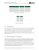
The Xilinx Kintex-7 Data Sheet: DC and AC Switching Characteristics (DS182) provides more information on the
power supply requirements of the FPGA board.
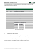
Supply
Derived From Application
5.0 V
12.0 V
USB HID; FMC
3.3 V 12.0 V
SD Card; Ethernet PHYs; Cypress FX2LP; Microchip PIC; BPI Flash;
FPGA I/O Banks 14,15; FMC; PMODs
2.0 V 5.0 V
FPGA auxiliary supply, VCC
BAT
; Backup battery; Real-time clock
backup.
1.8 V
12.0 V
QDRII+ supply
1.8 V
3.3 V
FPGA GTX transceiver Quad PLL
1.5 V
12.0 V
DDR3; FPGA I/O Bank 34
1.2 V
12.0 V
FPGA GTX transceiver termination
1.0 V
12.0 V
FPGA GTX analog supply
1.0 V
3.3 V
FPGA Core
0.9 V
3.3 V
QDRII+ reference
0.75 V
3.3 V
DDR3 reference
VADJ 12.0 V
FPGA I/O Banks 12, 13; FMC; Configurable.
SET_VADJ2
FPGA AF20
SET_VADJ1
FPGA AF19
VADJ
0
0
1.2 V
0
1
1.8 V
1
0
2.5 V
1
1
3.3 V
Table 1. On-board power supplies.
3 Oscillators and Clocks
On-board oscillators support various board subsystems. A low-jitter 125 MHz oscillator is provided for the Ethernet
PHYs and a 50 MHz oscillator drives the FPGA master configuration clock. The Cypress FX2LP and Microchip PIC
microcontrollers each contain on-chip oscillators running at 24 MHz and 8 MHz, respectively.
The main FPGA system clock is provided by an ultra-low-jitter 200 MHz differential oscillator connected to pins
AA2 and AA3 in I/O bank 34. This can drive up to ten internal PLLs (Phase Locked Loops) and MMCMs (Mixed-
Mode Clock Managers) on the FPGA for high-performance multi-clock-domain designs. Please refer to the Xilinx 7-
series Clock Resources User Guide (UG472) for more details on FPGA internal clocking resources.
Copyright Digilent, Inc. All rights reserved.
Other product and company names mentioned may be trademarks of their respective owners.
Page 6 of 26