Opus Card Reference Manual Reference Manual (v1.
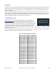
Table of Contents 1 SUMMARY OF FEATURES.......................................................................................................................................... 3 Figure 1-1: Opus Card............................................................................................................................................................................ 3 2 OVERVIEW............................................................................................................................
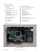
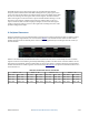
1 Summary of Features • Onboard Xilinx Virtex-5 FPGA • Secure Digital File System ◦ Model: FX30T ▪ PowerPC and MicroBlaze cores ▪ Hard Ethernet MAC ◦ Includes a 2 GB SD card configured with Linux image that runs on the PowerPC core • External Connectors • Programmable Clock Generator Chip ◦ Model: IDT 5V9885 ▪ 8 outputs with available frequencies from 0.
2 Overview The Opus card is a complete development system driven by the Xilinx Virtex 5 FPGA. The card was designed with the end-purpose of running as a standalone Linux system that plugs into a host PC and is a node in a network of Opus systems. In addition to the node functionality, the Opus card also has all the necessary components to be an independent development platform.
3 Power Supply The Opus card requires a 12V 6-pin PCIe expansion card power source, available on most modern power supply units. The socket on the card is white in color and located in the upper right corner of the card, labeled as J6. The power supply should be switched off while plugging in the Opus card. 4 FPGA and Platorm Flash Confguraton The Opus card must be configured before use.
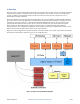
Memory The Opus has a total of 256 MB of DDR-2 RAM, divided into two banks of 128 MB. Each bank is organized into 32 bit words, which can be written and read in bursts by enabling burst mode. In big endian format, writing a 1 to the 31 st bit of the configuration register enables burst mode. The configuration register for each bank is located at the base address of the registers. The Opus card also has 32 Mb of platform flash, which can store hardware bitstreams between power cycles.
The GPIO pins have an I/O level of 3.3V. They are controlled using the General Purpose I/O IP included with the Xilinx EDK. Adding the IP to a project gives access to two sets of two 32-bit software accessible registers at the base address of the GPIO IP, each set consisting of a data register and a tri-state register. Each bit in the data and tri-state register can be connected to a pin on the GPIO header.