
Instruction Manual


XUP Virtex-II Pro Development System www.xilinx.com 67
UG069 (v1.0) March 8, 2005
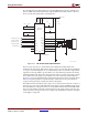
Using the Multi-Gigabit Transceivers
R
Using the Multi-Gigabit Transceivers
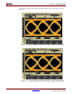
The embedded RocketIO™ multi-gigabit transceiver core is based on Mindspeed’s
SkyRail™ technology. Eight transceiver cores are available in each of the FPGAs that can be
used on the XUP Virtex-II Pro Development System.
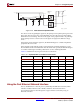
The transceiver core is designed to operate at any baud rate in the range of 622 Mb/s to
3.125 Gb/s per channel. Only four of the available eight channels are used on the XUP
Virtex-II Pro Development System. Three channels are equipped with low-costs Serial
Advanced Technology Attachment (SATA) connectors and the fourth channel terminates
at user-supplied Sub-Miniature A (SMA) connectors. The SATA channels are split into two
interface formats, two HOST ports (J16, J18), and a TARGET port (J17). The TARGET port
interchanges the transmit and receive differential pairs to allow two XUP Virtex-II Pro
Development Systems to be connected as a simple network, or multiple XUP Virtex-II Pro
Development Systems to be connected in a ring. The SATA specification requires an out-of-
band signalling state that is to be used when the channel is idle. This capability is not
directly provided by the MGTs. Two resistors, an FET transistor, and two AC coupling
capacitors along with special idle state control signals add the out-of-band IDLE state
signaling capability to the MTGs. Additional off-board hardware can be required to
properly interface to generic SATA disk drives.
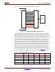
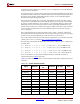
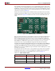
CF_MPD[3] I/O 62 AF14 LVCMOS25 8 mA
CF_MPD[4] I/O 61 AE14 LVCMOS25 8 mA
CF_MPD[5] I/O 60 AD14 LVCMOS25 8 mA
CF_MPD[6] I/O 59 AC15 LVCMOS25 8 mA
CF_MPD[7] I/O 58 AB15 LVCMOS25 8 mA
CF_MPD[8] I/O 56 AJ9 LVCMOS25 8 mA
CF_MPD[9] I/O 53 AH9 LVCMOS25 8 mA
CF_MPD[10] I/O 52 AE10 LVCMOS25 8 mA
CF_MPD[11] I/O 51 AE9 LVCMOS25 8 mA
CF_MPD[12] I/O 50 AD12 LVCMOS25 8 mA
CF_MPD[13] I/O 49 AC12 LVCMOS25 8 mA
CF_MPD[14] I/O 48 AG10 LVCMOS25 8 mA
CF_MPD[15] I/O 47 AF10 LVCMOS25 8 mA
CF_MP_CE_Z O 42 AB16 LVCMOS25 8 mA
CF_MP_OE_Z O 77 AD17 LVCMOS25 8 mA
CF_MP_WE_Z O 76 AC16 LVCMOS25 8 mA
CF_MPIRQ I 41 AD16 LVCMOS25 -
CF_MPBRDY I 39 AE16 LVCMOS25 -
Table 2-20: System ACE Connections (Continued)
Signal Direction
System ACE
Pin
FPGA Pin I/O Type Drive