
Instruction Manual

XUP Virtex-II Pro Development System www.xilinx.com 59
UG069 (v1.0) March 8, 2005
Using the CPU Debug Port and CPU Reset
R
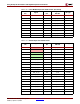
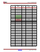
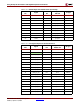
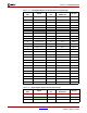
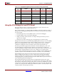
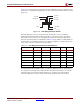
Figure 2-15 shows the pinout of the header used to debug the operation of software in the
CPU. This is accomplished using debug tools, such as the Xilinx Parallel Cable IV or third
party tools.
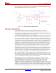
The JTAG debug resources are not hardwired to specific pins and are available for
attachment in the FPGA fabric, making it possible to route these signals to whichever
FPGA pins the user prefers to use. The signal-pin connections used on the XUP Virtex-
II Pro Development System are identified in Table 2-17 along with the recommended I/O
characteristics. Level shifting circuitry is provided for all signals to convert from the 3.3V
levels at the connector to the 2.5V levels at the FPGA.
The RESET_RELOAD pushbutton (SW1) provides two different functions depending on
how long the switch is depressed. If the switch is activated for more than 2 seconds, the
XUP Virtex-II Pro Development System undergoes a complete reset and reloads the
selected configuration. If, however, the switch is activated for less than 2 seconds, a
Figure 2-15: CPU Debug Connector Pinouts
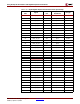
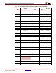
Table 2-17: CPU Debug Port Connections and CPU Reset
Signal Direction FPGA Pin I/O Type DRIVE Slew
PROC_RESET_Z I AH5 LVTTL – –
CPU_TDO O AG16 LVCMOS25 12 mA SLOW
CPU_TDI I AF15 LVCMOS25 – –
CPU_TMS I AJ16 LVCMOS25 – –
CPU_TCK I AG15 LVCMOS25 – –
CPU_TRST I AC21 LVCMOS25 – –
CPU_HALT_Z I AJ23 LVCMOS25 – –
15 1
2
16
CPU TMS
CPU HALT Z
GND
CPU TCK
CPU TDO
CPU TRST
3.3V
CPU TDI
UG069_15_082404