
Instruction Manual

XUP Virtex-II Pro Development System www.xilinx.com 43
UG069 (v1.0) March 8, 2005
Using the LEDs and Switches
R
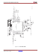
The FPGA contains the AC97 controller that provides control information and PCM data
on the outbound link and receives status information and PCM data in the inbound link.
The complete AC97 interface consists of four signals, the clock AC97_BIT_CLOCK, a
synchronization pulse AC97_SYNCH, and the two serial data links AC97_SDATA_IN and
AC97_SDATA_OUT listed in Table 2-8.
The CODEC is held in a reset state until the AUDIO_RESET_Z signal is driven high by the
FPGA overriding a pull-down resistor (R15).
Using the LEDs and Switches
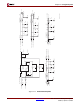
The XUP Virtex-II Pro Development System includes four LEDs as visual indicators for the
user to define, as well as four DIP switches and five pushbuttons for user-defined use. The
pushbuttons are arranged in a diamond shape with the ENTER pushbutton in the center of
the diamond. This placement can be used for object movement in a game. None of the DIP
switches or pushbuttons have external de-bouncing circuitry, because this should be
provided in the FPGA application. Table 2-9 identifies the connections between the user
switches, user LEDs, and the FPGA.
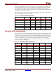
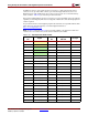
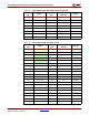
Table 2-8: AC97 Audio CODEC Connections
Signal Direction FPGA Pin I/O Type Drive Slew
AC97_SDATA_OUT O E8 LVTTL 8 mA SLOW
AC97_SDATA_IN I E9 LVTTL – –
AC97_SYNCH O F7 LVTTL 8 mA SLOW
AC97_BIT_CLOCK I F8 LVTTL – –
AUDIO_RESET_Z O E6 LVTTL 8 mA SLOW
BEEP_TONE_IN O E7 LVTTL 8 mA SLOW
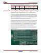
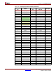
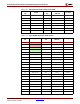
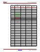
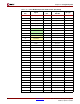
Table 2-9: User LED and Switch Connections
Signal Direction FPGA Pin I/O Type Drive Slew
LED_0 O AC4 LVTTL 12 mA SLOW
LED_1 O AC3 LVTTL 12 mA SLOW
LED_2 O AA6 LVTTL 12 mA SLOW
LED_3 O AA5 LVTTL 12 mA SLOW
SW_0 I AC11 LVCMOS25 – –
SW_1 I AD11 LVCMOS25 – –
SW_2 I AF8 LVCMOS25 – –
SW_3 I AF9 LVCMOS25 – –
PB_ENTER I AG5 LVTTL – –
PB_UP I AH4 LVTTL – –
PB_DOWN I AG3 LVTTL – –