
Instruction Manual

34 www.xilinx.com XUP Virtex-II Pro Development System
UG069 (v1.0) March 8, 2005
Chapter 2: Using the System
R
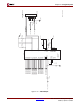
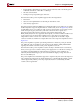
Using the XSGA Output
The XSGA output on the XUP Virtex-II Pro Development System is made up from a triple
8-bit DAC (U29), a high density 15-pin D-Sub connector (J13), and IP placed in the FPGA
fabric. The FMS3818 video DAC is a low-cost DAC tailored to fit graphics and video
applications, with a maximum pixel clock of 180 MHz. The TTL data inputs and control
signals are converted into analog current outputs that can drive 25Ω to 37.5Ω loads,
corresponding to a doubly-terminated 50Ω to 75Ω load. The VGA_OUT_BLANK_Z input
overrides the RGB inputs and blanks the display output. This signal is equipped with a
pull-down resistor (R120) to keep the display blanked when the FPGA is not programmed
or XSGA output is not required by the user application. The XSGA output circuit is shown
in Figure 2-11.
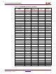
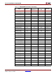
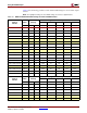
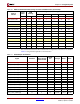
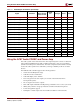
SDRAM_A[13] O 167 M23 SSTL2-II
SDRAM_CK0 O 137 AC27 SSTL2-II
SDRAM_CK0_Z O 138 AC28 SSTL2-II
SDRAM_CK1 O 16 AD29 SSTL2-II
SDRAM_CK1_Z O 17 AD30 SSTL2-II
SDRAM_CK2 O 76 AB23 SSTL2-II
SDRAM_CK2_Z O 75 AB24 SSTL2-II
CLK_FEEDBACK O – G23 LVCMOS25
CLK_FEEDBACK I – C16 LVCMOS25
SDRAM_CKE0 O 21 R26 SSTL2-II
SDRAM_CKE1 O 111 R25 SSTL2-II
SDRAM_RAS_Z O 154 N29 SSTL2-II
SDRAM_CAS_Z O 65 L27 SSTL2-II
SDRAM_WE_Z O 63 N26 SSTL2-II
SDRAM_S0_Z O 157 R24 SSTL2-II
SDRAM_S1_Z O 158 R23 SSTL2-II
SDRAM_BA0 O 59 M26 SSTL2-II
SDRAM_BA1 O 52 K26 SSTL2-II
SDRAM_SDA I/O 91 AF23 LVCMOS25
SDRAM_SCL O 92 AF22 LVCMOS25
SDRAM_SA0 NA 181 – NA
SDRAM_SA1 NA 182 – NA
SDRAM_SA2 NA 183 – NA
Table 2-5: DDR SDRAM Connections (Continued)
Signal Direction
DIMM
Module Pin
FPGA
Pin
I/O Type