
Instruction Manual

30 www.xilinx.com XUP Virtex-II Pro Development System
UG069 (v1.0) March 8, 2005
Chapter 2: Using the System
R
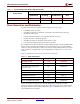
Xilinx has qualified several different types of PC2100 memory modules for use in the XUP
Virtex-II Pro Development System. These modules cover various densities, organizations,
and features. The qualified memory modules are identified in Table 2-4.
For an updated list of supported modules, consult the XUP Virtex-II Pro Development
System support Web site at:
http://www.xilinx.com/univ/xupv2p.html
The data bus width, number of ranks, address range, clock latency, and output type are all
parameters that are used by the DDR memory controller design to create the correct
memory controller for the user application.
These memory modules are designed for a maximum clock frequency of at least 133 MHz
and have a CAS latency of 2.5 (18.8 ns). The PLB Double Data Rate Synchronous DRAM
Controller supports CAS latencies of two or three clock cycles.
If the memory system is to operate at 100 MHz, then set the CAS latency parameter in the
controller design to 2 (20 ns). If full speed (133MHz) memory operation is required, then
set the CAS latency parameter in the controller design to 3 (22.6 ns).
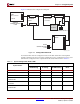
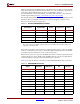
Table 2-5 provides the details on the FPGA to DDR SDRAM DIMM module connections.
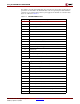
Table 2-4: Qualified SDRAM Memory Modules
Crucial® Technology
Part Number
Memory
Organization
Number of
Ranks
Unbuffered or
Registered
CAS
Latency
CT6472Z265.18T* 512 MB 64M X 72 Dual Unbuffered 2.5
CT6464Z265.16T* 512 MB 64M X 64 Dual Unbuffered 2.5
CT6472Z265.9T* 512 MB 64M X 72 Single Unbuffered 2.5
CT6464Z265.8T* 512 MB 64M X 64 Single Unbuffered 2.5
CT1664Z265.4T* 128 MB 16M X 64 Single Unbuffered 2.5
Notes:
The * in the Crucial part number represents the revision number of the module, which is not
required to order the module.
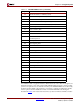
Table 2-5: DDR SDRAM Connections
Signal Direction
DIMM
Module Pin
FPGA
Pin
I/O Type
SDRAM_DQ[0] I/O 2 C27 SSTL2-II
SDRAM_DQ[1] I/O 4 D28 SSTL2-II
SDRAM_DQ[2] I/O 6 D29 SSTL2-II
SDRAM_DQ[3] I/O 8 D30 SSTL2-II
SDRAM_DQ[4] I/O 94 H25 SSTL2-II
SDRAM_DQ[5] I/O 95 H26 SSTL2-II
SDRAM_DQ[6] I/O 98 E27 SSTL2-II
SDRAM_DQ[7] I/O 99 E28 SSTL2-II
SDRAM_DQS[0] I/O 5 E30 SSTL2-II
SDRAM_DM[0] 0 97 U26 SSTL2-II