
Instruction Manual

28 www.xilinx.com XUP Virtex-II Pro Development System
UG069 (v1.0) March 8, 2005
Chapter 2: Using the System
R
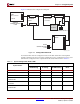
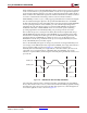
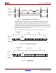
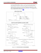
The DIMM module is supplied with three differential clocks. These three clock signals are
matched in length to each other and the DDR SDRAM feedback signals to allow for fully
synchronous operation across all banks of memory. The DDR SDRAM clocks are driven by
Double Data Rate (DDR) output registers, connected to a Digital Clock Manager (DCM)
with an optional external feedback connection. The DDR SDRAM controller logic is
described in DS425
, PLB Double Data Rate (DDR) Synchronous DRAM (SDRAM) Controller.
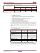
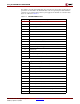
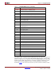
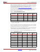
29 Minimum RAS# to CAS# delay (trcd)
30 Minimum RAS# pulse width (tras)
31 Module rank density
32 Command and address setup time (tas, tcms)
33 Command and address hold time (tah, tcmh)
34 Data setup time (tds)
35 Data hold time (tdh)
36-40 Reserved
41 Minimum ACTIVE/AUTO REFRESH time
42 Minimum AUTO REFRESH to ACTIVE/AUTO REFRESH
command period
43 Max cycle time
44 Max DQS-DQ skew
45 Max READ HOLD time
46 Reserved
47 DIMM height
48-61 Reserved
62 SPD revision
63 CHECKSUM for bytes 0-62
64-71 Manufacturer's JEDEC ID code
72 Manufacturing location
73-90 Module part number (ASCII)
91-92 Module revision code
93 Year of manufacture (BCD)
94 Week of manufacturer (BCD)
95-98 Module serial number
99-127 Reserved
128-255 User defined contents
Table 2-3: SPD EEPROM Contents (Continued)
Byte Description