
Instruction Manual

XUP Virtex-II Pro Development System www.xilinx.com 27
UG069 (v1.0) March 8, 2005
Using the DIMM Module DDR SDRAM
R
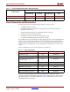
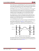
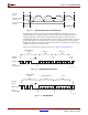
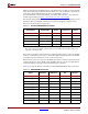
The ability to read the SPD EEPROM is important because the module specific timing
parameters are included in the EEPROM data and are required by the DDR SDRAM
controller to provide the highest memory throughput. The definitions of the SPD data
bytes are outlined in Table 2-3.
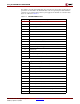
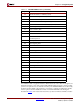
Table 2-3: SPD EEPROM Contents
Byte Description
0 Number of used bytes in SPD EEPROM
1 Total number of bytes on SPD EEPROM
2 Memory type (DDR SDRAM = 07h)
3Number of row addresses
4 Number of column addresses
5 Number of ranks (01h)
6-7 Module data width
8 Module interface voltage (SSTL 2.5V = 04h)
9 SDRAM cycle time (tck) (CAS LATENCY = 2.5)
10 SDRAM access time (tac) (CAS LATENCY = 2.5)
11 Module configuration type
12 Refresh rate
13 Primary SDRAM component width
14 Error checking SDRAM component width
15 Minimum clock delay from
Back-to-Back Random Column Addresses
16 Supported burst lengths
17 Number of banks on SDRAM component
18 CAS latencies supported
19 CS latency
20 WE latency
21 SDRAM module attributes
22 SDRAM attributes
23 SDRAM cycle time (tck) (CAS LATENCY =2)
24 SDRAM access time (tac) (CAS LATENCY =2)
25 SDRAM cycle time (tck) (CAS LATENCY =1)
26 SDRAM access time (tac) (CAS LATENCY =1)
27 Minimum ROW PRECHARGE time (trp)
28 Minimum ROW ACTIVE to ROW ACTIVE (trrd)