
Instruction Manual

XUP Virtex-II Pro Development System www.xilinx.com 23
UG069 (v1.0) March 8, 2005
Clock Generation and Distribution
R
Clock Generation and Distribution
The XUP Virtex-II Pro Development System supports six clock sources:
• A 100 MHz system clock (Y2),
• A 75 MHz clock (U10) for the MGTs operating the Serial Advanced Technology
Attachment (SATA) ports,
• A dual footprint through-hole user-supplied alternate clock (Y3),
• An external clock for the MGTs (J23-J24),
• A 32 MHz clock (Y4) for the System ACE interfaces, and
• A clock from the Digilent high-speed expansion module.
The 75 MHz SATA clock is obtained from a high stability (20 ppm) 3.3V LVDSL differential
output oscillator, and the external MGT clock is obtained from two user-supplied SMA
connectors. The remaining three oscillators are all 3.3V single-ended LVTTL sources. Each
of the oscillators is equipped with a power supply filter to reduce the noise on the clock
outputs.
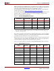
Table 2-2 identifies the various clock connections for the FPGA.
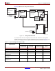
For the user to take advantage of the external differential clock inputs, two SMA
connectors must be installed at J23 and J24. These SMA connectors can be purchased from
Digi-Key® under the part number A24691-ND. Figure 2-4 identifies the location of the
external differential clock inputs.
JTAG USB or PC4 LOADING OFF ON OFF OFF
JTAG USB or PC4 COMPLETED OFF ON OFF ON
Table 2-1: System Configuration Status LEDs (Continued)
System Status
LED Status
D19 (Green)
PROM Config
D20 (Green)
CF Config
D14 (Amber)
GOLDEN Config
D4 (Red)
Done
Table 2-2: Clock Connections
Signal FPGA Pin I/O Type
SYSTEM_CLOCK AJ15 LVCMOS25
ALTERNATE_CLOCK AH16 LVCMOS25
HS_CLKIN (from high speed
expansion port)
B16 LVCMOS25
MGT_CLK_P F16 LVDS_25
MGT_CLK_N G16 LVDS_25
EXTERNAL_CLOCK_P G15 LVDS_25
EXTERNAL_CLOCK_N F15 LVDS_25
FPGA_SYSTEMACE_CLOCK AH15 LVCMOS25