
Instruction Manual

16 www.xilinx.com XUP Virtex-II Pro Development System
UG069 (v1.0) March 8, 2005
Chapter 1: XUP Virtex-II Pro Development System
R
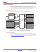
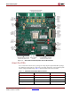
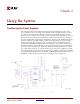
Figure 1-3 identifies the I/O banks that are used to connect the various peripheral devices
to the FPGA.
Power Supplies and FPGA Configuration
The XUP Virtex-II Pro Development System is powered from a 5V regulated power supply.
On-board switching power supplies generate 3.3V, 2.5V, and 1.5V for the FPGA, and
peripheral components and linear regulators power the MGTs.
The board has provisioning for current measurement for all of the FPGA digital power
supplies, as well as application of external power if the capacity of the on-board switching
power supplies is exceeded.
The XUP Virtex-II Pro Development System provides several methods for the
configuration of the Virtex-II Pro FPGA. The configuration data can originate from the
internal Platform Flash PROM (two potential configurations), the internal CompactFlash
storage media (eight potential configurations), and external configurations delivered from
the embedded Platform Cable USB or parallel port interface.
Block RAMs 1584 Kb 2448 Kb
DCMs 8 8
PowerPC RISC Cores 2 2
Multi-Gigabit Transceivers 8 8
Figure 1-3: I/O Bank Connections to Peripheral Devices
Table 1-1: XC2VP20 and XC2VP30 Device Features (Continued)
Features XC2VP20 XC2VP30
10/100 Ethernet
AC97 Audio SXGA port
System ACE port
LEDs & SWITCHES
PS/2 KBD & MOUSE
PUSH BUTTONS
RS-232
3.3V IO
EXPANSION CONNECTORS
OVER VOLTAGE CLAMPS
256M x 64/72 DDR SDRAM DIMM MODULE
1
2
3
7
6
0
45
UG069_03_012105
2.5V IO