
User Manual


1-Aug-2012
8
CLK3) are used to represent the Micron device electrically furthest from 7Z020 (IC25). The
worksheet calculation results are shown in the following table.
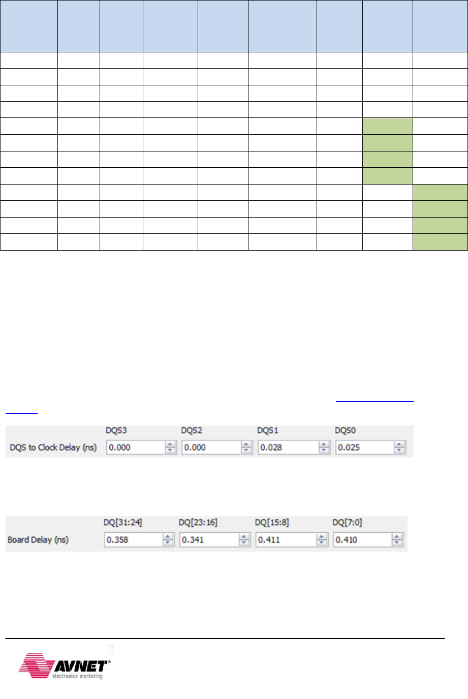
Table 2 - DDR3 Worksheet Calculations
Pin Group
Length
(mm)
Length
(mils)
Package
Length
(mils)
Total
Length
(mils)
Propagation
Delay
(ps/inch)
Total
Delay
(ns)
DQS to
CLK
Delay
(ns)
Board
Delay
(ns)
CLK0
55.77
2195.9
470
2665.9
160
0.427
CLK1
55.77
2195.9
470
2665.9
160
0.427
CLK2
41.43
1631.1
470
2101.1
160
0.336
CLK3
41.43
1631.1
470
2101.1
160
0.336
DQS0
51.00
2008.0
504
2512.0
160
0.402
0.025
DQS1
50.77
1998.8
495
2493.8
160
0.399
0.028
DQS2
41.59
1637.6
520
2157.6
160
0.345
-0.009
DQS3
41.90
1649.4
835
2484.4
160
0.398
-0.061
DQ[7:0]
50.63
1993.3
465
2458.3
160
0.393
0.410
DQ[15:8]
50.71
1996.4
480
2476.4
160
0.396
0.411
DQ[23:16]
40.89
1609.9
550
2159.9
160
0.346
0.341
DQ[31:24]
40.58
1597.8
780
2377.8
160
0.380
0.358
The DQS to CLK Delay fields in the PS7 DDR Configuration window should be populated using
the corresponding values from the previous table.
The configuration fields of the tool may not allow you to input a negative delay value, this is a
known problem with the 14.1 tools and scheduled for correction in the 14.2 tools release. In the
case of DQS2 and DQS3 fields for DQS to CLK Delay, simply enter a value of zero rather than
the negative delay values. This is an acceptable workaround since the calculated values are
relatively close to zero and the values provided in these fields are used as initial values for the
read/write training for DDR3. Keep in mind for LPDDR2 there is no write leveling, and for DDR2
there is no training whatsoever. In these memory use cases, the accuracy of the trace length info
is more important. This is covered in further detail in section 10.6.8 of the Xilinx Zynq TRM,
UG585.
Figure 3 - DQS to Clock Delay Settings
The Board Delay fields in the PS7 DDR Configuration window should be populated using the
corresponding values from the table above.
Figure 4 - DDR3 Board Delay Settings