ZedBoard Zynq™ Evaluation and Development Hardware User’s Guide Version 1.
Revision History Rev date 8/1/12 8/2/12 Rev # 1.0 1.
Table of Contents 1 INTRODUCTION .................................................................................................................................. 3 1.1 2 ZYNQ BANK PIN ASSIGNMENTS ...................................................................................................... 5 FUNCTIONAL DESCRIPTION ............................................................................................................ 6 2.1 EPP ...............................................................
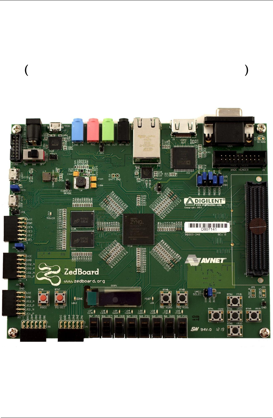
1 Introduction The ZedBoard is an evaluation and development board based on the Xilinx Zynq-7000 Extensible Processing Platform. Combining a dual Corex-A9 Processing System (PS) with 85,000 Series-7 Programmable Logic (PL) cells, the Zynq-7000 EPP can be targeted for broad use in many applications. The ZedBoard’s robust mix of on-board peripherals and expansion capabilities make it an ideal platform for both novice and experienced designers.
7 Flash QSPI QSPI 32 PMOD Gbit Enet 14 ENET/ MDIO USB OTG PHY 12 PHY USBOTG 8 SD USB UART USB Cont 2 Pmods 82 FMC MIO 8 Pmod GPIO FMC-LPC SD HdPhn Out USBUART 8 I2S/ACD Line Out Line In MIC In PL PS_GPIO 27 HDMI 1 DDR VGA PS 71 DDR3 Reset 33Mhz I2S Audio Codec 3 1 LED, 2 buttons 512Mbyte DDR3 (x32) GPIO (8 LEDs, 8 slide switches, 5 pushbuttons) 21 OLED PS_RST DONE Clk 1 PS_CLK PROG GPIO/VP/VN JTAG HDMI transmitter 10 5 VGA (12bit color
1.1 Zynq Bank Pin Assignments The following figure shows the Zynq bank pin assignments on the ZedBoard followed by a table that shows the detailed I/O connections. .
2 Functional Description 2.1 EPP The ZedBoard features a Xilinx Zynq XC7Z020-1CSG484 EPP. The initial ZedBoards ship with Engineering Sample "CES" grade silicon. Later shipments will eventually switch to production "C" grade silicon once they become available. The EPP part markings indicate the silicon grade. 2.2 Memory Zynq contains a hardened PS memory interface unit. The memory interface unit includes a dynamic memory controller and static memory interface modules. 2.2.
The PCB design guidelines outlined in Zynq datasheet must be followed for trace matching, etc.
CLK3) are used to represent the Micron device electrically furthest from 7Z020 (IC25). The worksheet calculation results are shown in the following table. Pin Group Length (mm) Table 2 - DDR3 Worksheet Calculations Length Package Total Propagation Total (mils) Length Length Delay Delay (mils) (mils) (ps/inch) (ns) CLK0 55.77 2195.9 470 2665.9 160 0.427 CLK1 55.77 2195.9 470 2665.9 160 0.427 CLK2 41.43 1631.1 470 2101.1 160 0.336 CLK3 41.43 1631.1 470 2101.1 160 0.
2.2.2 SPI Flash The ZedBoard features a 4-bit SPI (quad-SPI) serial NOR flash. The Spansion S25FL256S is used on this board. The Multi-I/O SPI Flash memory is used to provide non-volatile code, and data storage. It can be used to initialize the PS subsystem as well as configure the PL subsystem (bitstream). Spansion provides Spansion Flash File System (FFS) for use after booting the Zynq EPP.
Two packages can be used on the ZedBoard; SO-16 and WSON. For the WSON package, there is a heat sink slug under the package that is not connected to any signal on the PCB.
2.2.3 SD Card Interface The Zynq PS SD/SDIO peripheral controls communication with the ZedBoard SD Card (A 4GB Class 4 card is included in the ZedBoard kit.) The SD card can be used for non-volatile external memory storage as well as booting the Zynq EPP. PS peripheral sd0 is connected through Bank 1/501 MIO[40-47], including, Card Detect and Write Protect. The SD Card is a 3.3V interface but is connected through MIO Bank 1/501 (1.8V). Therefore, a TI TXS02612 level shifter performs this translation.
2.3 USB 2.3.1 USB OTG ZedBoard implements one of the two available PS USB OTG interfaces. An external PHY with an 8-bit ULPI interface is required. A TI TUSB1210 Standalone USB Transceiver Chip is used as the PHY. The PHY features a complete HS-USB Physical Front-End supporting speeds of up to 480Mbs. This part is available in a 32-pin QFN package. VCCio for this device is 1.8V and cannot be connected through level shifters. The PHY is connected to MIO Bank 1/501, which is powered at 1.8V.
This USB port will not power the board. Therefore, Vbus needs to be connected to 3.3V though a 1KΩ series resistor. The Wake pin, pin 22, connects to GND. A 24Ω series resistor was placed on each of the data lines, D+ and D-. EPP Pin D11 (MIO Bank 1/501) C14 (MIO Bank 1/501) Table 6 – CY7C6 Connections UART Function in Schematic Net CY7C6 Pin EPP Name UART Function in CY7C64225 TX, data out USB_1_RXD 23 RXD, data in RX, data in USB_1_TXD 4 TXD, data out Figure 7 – USB-UART Bridge Interface 2.3.
2.3.4 USB circuit protection All USB data lines, D+/-, are protected with a TE SESD0402Q2UG-0020-090. D+ D- Level Shifter USB Con n Figure 8 – ESD Protection 2.4 2.4.1 Display and Audio HDMI Output An Analog Devices ADV7511 HDMI Transmitter provides a digital video interface to the ZedBoard. This 225MHz transmitter is HDMI 1.4- and DVI 1.0-compatible supporting 1080p60 with 16-bit, YCbCr, 4:2:2 mode color. The ADV7511 supports both S/PDIF and 8-channel I2S audio.
Signal Name HDP HD-INT HD-SCL HD-SDA HD-CLK HD-VSYNC HD-HSYNC HD-DE HD_D[15:0] HD-SPDIF HD-SPDIFO Table 7 - HDMI Interface Connections Description Zynq EPP pin Hot Plug Detect signal input N/C Interrupt signal output W16 I2C Interface. Supports CMOS AA18 logic levels from 1.8V to 3.3V Y16 Video Clock Input. Supports typical CMOS logic levels from 1.8V up to 3.
Figure 9 - HDMI Video Interface Timing The HDMI transmitter connects externally via a HDMI Type A connector, J9, TE 1903015-1. Circuit protection for the HDMI interface is provided by a Tyco Electronics SESD0802Q4UG.
2.4.2 VGA Connector The ZedBoard also allows 12-bit color video output through a through-hole VGA connector, TE 41734682-2. Each color is created from resistor-ladder from four PL pins.
2.4.3 I2S Audio Codec An Analog Devices ADAU1761 Audio Codec provides integrated digital audio processing to the EPP. It allows for stereo 48KHz record and playback. Sample rates from 8KHz to 96KHz are supported. Additionally, the ADAU1761 provides digital volume control. The Codec can be configured using Analog Devices SigmaStudio™ for optimizing audio for specific acoustics, numerous filters, algorithms and enchancements. Analog Devices provides Linux drivers for this device. http://www.analog.
2.4.4 OLED An Inteltronic/Wisechip UG-2832HSWEG04 OLED Display is used on the ZedBoard. This provides a 128x32 pixel, passive-matrix, monochrome display. The display size is 30mm x 11.5mm x 1.45mm.
2.6.2 Program Push Button Switch A PROG push switch, BTN6, toggles EPP PROG_B. This initiates reconfiguring the PLsubsection by the processor. 2.6.3 Processor Subsystem Reset Power-on reset, labeled PS_RST/BTN7, erases all debug configurations. The external system reset allows the user to reset all of the functional logic within the device without disturbing the debug environment. For example, the previous break points set by the user remain valid after system reset.
2.7.3 User LEDs The ZedBoard has eight user LEDs, LD0 – LD7. A logic high on the EPP I/O causes the LED to turn on. LED’s are sourced from 3.3V banks through 390Ω resistors. Table 14 - LED Connections Signal Name Zynq EPP pin LD0 T22 LD1 T21 LD2 U22 LD3 U21 LD4 V22 LD5 W22 LD6 U19 LD7 U14 2.8 10/100/1000 Ethernet PHY The ZedBoard implements a 10/100/1000 Ethernet port for network connection using a Marvell 88E1518 PHY. This part operates at 1.8V. The PHY connects to MIO Bank 1/501 (1.
Table 15 – Ethernet PHY Pin Assignment and Definitions Signal Name Description Zynq EPP pin 88E1510 pin RX_CLK Receive Clock A14 40 RX_CTRL Receive Control D7 37 Receive Data RXD0: E11 38 RXD1: B7 39 RXD[3:0] RXD2: F12 41 RXD3: A13 42 TX_CLK Transmit Clock D6 47 TX_CTRL Transmit Control F11 2 Transmit Data TXD0: E9 44 TXD1: A7 45 TXD[3:0] TXD2: E10 48 TXD3: A8 1 MDIO Management Data C12 5 MDC Management Clock D10 4 The datasheet for the Marvell 88E1518 is not available publicly.
2.9.2 Digilent Pmod™ Compatible Headers (2x6) The ZedBoard has five Digilent Pmod™ compatible headers (2x6). These are right-angle, 0.1” female headers that include eight user I/O plus 3.3V and ground signals as show in the figure below. Four Pmod connectors interface to the PL-side of the EPP. These will connect to EPP Bank 13 (3.3V). One Pmod, JE1, connects to the PS-side of the EPP on MIO pins [7,9-15] in EPP MIO Bank 0/500 (3.3V).
Pmod JA1 Pmod JC1 Differential Table 16 - Pmod Connections Pmod Zynq EPP pin Signal Name Signal Name JA1 JA2 JA3 JA4 JA7 JA8 JA9 JA10 Y11 AA11 Y19 AA9 AB11 AB10 AB9 AA8 JB1 Signal Name Zynq EPP pin JC1_N JC1_P JC2_N JC2_P JC3_N JC3_P JC4_N JC4_P AB6 AB7 AA4 Y4 T6 R6 U4 T4 Pmod JE1 MIO Pmod JB1 JB2 JB3 JB4 JB7 JB8 JB9 JB10 Pmod Signal Name JD1 Differential Signal Name JE1 JE2 JE3 JE4 JE7 JE8 JE9 JE10 JD1_N JD1_P JD2_N JD2_P JD3_N JD3_P JD4_N JD4_P Zynq EPP pin W12 W11 V10 W8 V12 W10 V9 V8
Figure 13 - Analog Header Pin out The following anti-aliasing filters were used for the XADC inputs: - VP/VN - VAUX0P/VAUX0N - VAUX8P/VAUX8N Figure 14 - Anti-Aliasing Filters for XADC Inputs 25 1-Aug-2012
Table 17 - Analog Header Pin Out Name VP/VN VAUX0P/VAUX0N Description Requirement XADC Header EPP Pin Two pins required. Dedicated pins on the 7 series package. 1V peak-topeak input 1 XADC-VN-R : M12 This is the dedicated analog input channel for the ADC(s). maximum 2 XADC-VP-R : L11 Two pins required. Auxiliary analog input channel 0. Two dedicated channels needed for simultaneous sampling applications.
2.10 Configuration Modes Zynq-7000 EPP devices use a multi-stage boot process that supports both non-secure and secure boot (note that secure boot is not supported for CES silicon.) The PS is the master of the boot and configuration process. The following table shows the Zynq configuration modes. Upon reset, the device mode pins are read to determine the primary boot device to be used: NOR, NAND, Quad-SPI, SD Card or JTAG. By default, the ZedBoard uses the SD Card configuration mode.
The PS boot mode selections are shown in the table below, default setting highlighted in yellow: Table 18 – ZedBoard Configuration Modes Xilinx TRM MIO[6] MIO[5] MIO[4] MIO[3] MIO[2] Boot_Mode[4] Boot_Mode[2] Boot_Mode[1] Boot_Mode[0] Boot_Mode[3] JTAG Mode Cascaded JTAG Independent JTAG 0 1 Boot Devices 0 0 1 0 1 1 PLL Mode JTAG Quad-SPI SD Card PLL Used PLL Bypassed 0 0 0 0 1 Bank Voltages MIO Bank 500 MIO Bank 501 3.3V 1.8V Expected configuration time using a 50MB/s QSPI flash is 250ms.
2.11 Power 2.11.1 Primary Power Input The board’s primary input is through a 12V barrel jack. A compatible AC/DC converter will have a 2.5mm inner diameter, 5.5mm outer diameter, center positive connection. The total power budget is based on 4A from an AC/DC wall wart supply. This rail is protected with a TE 0603SFF600F/24-2. A 10mΩ, 1W current sense resistor exists in series with the 12V input power supply.
The table below shows the minimum required voltage rails, currents, and tolerances. Table 19 - TPS65708 Connections Voltage (V) Current (A) Tolerance 1.0 (Vccint) 1.3 5.00% 1.5 (Vccoddr) 1.5 5.00% 1.8 (Vccaux) 0.8 5.00% 1.8, 2.5, 3.3 (jumper adjustable, 2.5V default) (Vadj) 2 5.00% 3.3 (Vcco/FMC/Pmod) 3 5.00% 1.8 (analog) (Vccadc) 0.15 5.00% 1.25 reference (Vrefp) 0.005 0.2%, 50ppm/ºC 0.75 (DDR3 Vtt) 1.5 5.00% 5.0 (Filtered for XADC) 0.15 5.00% 2.11.
2.11.5 Power Good LED A green status LED, LD13, indicates when power is good on the board. Power Good is wired with the Resets and PROG to prevent operation of the board when power is not good. 2.11.6 Power Estimation The Power estimation chart is shown below. Table 20 – Current Usage Estimations, in mA Feature EPP PS EPP PL DDR3 DDR3 Termination QSPI Flash QSPI Flash 10/100/1000 PHY 10/100/1000 PHY USB 2.
Tolerance o 1.0V Vccint 0.95 to 1.05V o Vccaux +/- 5% o Vcco +/-5% Ramp time o 0.20 to 50ms o In-rush current must be controlled so the power circuitry is not overloaded at start-up Monotonicity o No negative dips in Vccint or Vccaux power-up ramps Sequencing o Verify sequencing responds as expected based on design Refer to Zynq Datasheet for the latest requirements 2.11.8 Probes Two ground test point are available on the board, J3 and J4.
3 Zynq EPP Banks The following figure and table show Zynq CLG484 I/O bank assignments on the Zynq board.
3.1 Zynq EPP Bank Voltages Table 21 - Zynq Bank Voltage Assignments EPP PS-Side Bank Voltage (default) MIO Bank 0/500 3.3V MIO Bank 1/501 1.8V DDR 1.5V EPP PL-Side Bank0 3.3V Bank 13 3.3V Bank 33 3.3V Bank 34 Vadj (2.5V) Bank 35 Vadj (2.5V) Note: Banks 34 and 35 are powered from an adjustable voltage rail. Jumper, J18, selects this voltage. Selectable voltages include 1.8V, 2.5V and 3.3V. The 3.
4 Jumper Settings Table 22 - Jumper Settings Ref Designator Description Default Setting JP1 Microphone Input Bias Open – No Electret Microphone JP2 Vbus 5V Enable JP3 USB Vbus Capacitor Setting JP4 CFGBVS Select Open JP5 PUDC Select Open JP6 PS_MIO0 Pull-Down Short Boot_Mode[3]/MIO[2] GND – Cascaded JTAG JP8 JP9 JP10 Boot_Mode[0]/MIO[3] Boot_Mode[1]/MIO[4] Boot_Mode[2]/MIO[5] 110 – SD Card JP11 Boot_Mode[4]/MIO[6] GND – PLL Used JP12 XADC Ferrite Bead Disable Open JP13 JTAG PS
Figure 20 - ZedBoard Jumper Map 36 1-Aug-2012
5 Mechanical The ZedBoard measures 6.3”x6.3”.