
User Manual


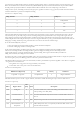


Offset Register Name
Size
[bits] R/W Description
0x04 Measured Fan Speed 16 R FPGA Fan Speed value in rpm, as computed based on the fan feedback pin.
Upon read, the low byte is received first.
0x06 Fan Speed Fault 8 8 Bits 7-1: Unused
Bit 0: ‘1’ if fan speed is outside the expected range; ‘0’ otherwise
0x07-
0x0E
Reserved for future
functionality
0x0F Platform MCU Control 8 R/W Bits 7-2: Unused
Bit 1: Fault Status:
- ‘1’ = Clear all faults
- [Default] ‘0’ = Do nothing
Once written with ‘1’, this bit returns by itself to ‘0’ after all the faults have
been cleared.
Bit 0: I2C Communication to PMUs Control:
- ‘1’ = I2C Communication to PMUs Disabled
- [Default] ‘0’ = I2C Communication to PMUs Enabled
0x10-
0x70
Reserved for future
functionality
When the PC wants to access a Platform MCU register, it needs to respect the following protocol:
It needs to send at first the address byte. Bits 7 to 1 of this byte contain the register start address (found in the first column from
Table 10.2.1.3). Bit 0 of this byte is logic ‘1’ for read transactions, and logic ‘0’ for write transactions.
It then needs to send a second byte, containing the number of bytes to read/write.
For write transactions, it then needs to send the actual values to be written in the Platform MCU registers. The number of bytes
sent in this phase needs to match the value from the previous byte (“the number of bytes to read/write”), otherwise
communication with the Platform MCU will hang.
For read transactions, the Platform MCU will then start to send the requested register values.
For write transactions, the maximum length is 256 bytes. After such a transaction, wait for a minimum of 100ms before sending a
new transaction (read or write) to the Platform MCU.
For consecutive write transactions, the total maximum length is 256 bytes. After such a transaction, wait for a minimum of 100ms
before sending a new transaction (read or write) to the Platform MCU.
All bytes to be sent to the PMCU need to have their nibbles converted to
ASCII () characters prior to being sent; e.g.: 0x0C in hex
needs to be converted to “0C” in ASCII ().
All characters received from the PMCU need to be converted from ASCII () to hex nibbles after being received; e.g. “0C” received
in ASCII () format needs to be converted to 0x0C in hex.
Write transaction example. Let’s say the PC wants to clear all system faults. For this, it will send to the Platform MCU:
Byte 0: 1E (i.e. Bits 7-1 = 0x0F which is the address of Platform MCU register; Bit 0 = ‘0’ meaning write transaction)
Byte 1: 01 (i.e. the PC want to write 1 byte)
Byte 2: 02 (value to write to register at address 0x0F - Clear all faults)
Read transaction example. Let’s say the PC wants to read Fan Speed Faults register from the Platform MCU. For this, it will send to the
Platform MCU:
Byte 0: 0D (i.e. Bits 7-1 = 0x06 which is the address of Fan Speed Fault register; Bit 0 = '1' meaning read transaction)
Byte 1: 01 (i.e. the PC wants to read 1 byte)
The Platform MCU will then send 1 byte back to the PC, containing the value of the Fan Speed Fault register.
To read a 16-bit register like Measured Fan Speed the PC will send to the Platform MCU:
Byte 0: 09 (i.e. Bits 7-1 = 0x04 which is the address of Measured Fan Speed register; Bit 0 = '1' meaning read transaction)
Byte 1: 02 (i.e the PC wants to read 2 bytes)
The Platform MCU will then send 2 bytes back to the PC. The first byte that is sent is the least significant one. If one receives 150C one
have to swap the first byte with the second one and to convert the value to decimal: 150C → 0x0C15 → 3093 RPM.
The UART baudrate should be set to 115200/8/E/1 (115200 baud, 8 data bits, even parity, 1 stop bit).