
Datasheet
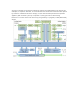

Signals in the Analog Input block, also called the Scope, use “SC” indexes to indicate they
are related to the scope block. Signals in theAnalog Output block, also called AWG, use
“AWG” indexes, and signals in the Digital block use a D index – all of the instruments
offered by the Discovery 2 and WaveForms use the circuits in these three blocks. Signal and
equations also use certain naming conventions. Analog voltages are prefixed with a “V” (for
voltage), and suffixes and indexes are used in various ways: to specify the location in the
signal path (IN, MUX, BUF, ADC, etc.); to indicate the related instrument (SC, AWG, etc.); to
indicate the channel (1 or 2); and to indicate the type of signal (P, N, or diff). Referring to the
block diagram in Fig. 2 below:
The Analog Inputs/Scope instrument block includes:
Input Divider and Gain Control: high bandwidth input adapter/divider. High or low-
gain can be selected by the FPGA
Buffer: high impedance buffer
Driver: provides appropriate signal levels and protection to the ADC. Offset voltage
is added for vertical position setting
Scope Reference and Offset: generates and buffers reference and offset voltages
for the scope stages
ADC: the analog-to-digital converter for both scope channels.
The Arbitrary Outputs/AWG instrument block includes:
DAC: the digital-to-analog converter for both AWG channels
I/V: current to bipolar voltage converters
Out: output stages
Audio: audio amplifiers for headphone
A precision Oscillator and a Clock Generator provide a high quality clock signal for the
AD and DA converters.
The Digital I/O block exposes protected access to the FPGA pins assigned for the
Digital Pattern Generator and Logic Analyzer.
The Power Supplies and Control block generates all internal supply voltages as well as
user supply programmable voltages. The control block also monitors the device power
consumption for USB compliance when power is supplied via the USB connection. When
external power supply is used, the control block allows more power for the user supplies.
Under the FPGA control, power for unused functional blocks can be turned off.
The USB Controller interfaces with the PC for programming the volatile FPGA memory
after power on or when a new configuration is requested. After that, it performs the data
transfer between the PC and FPGA.
The Calibration Memory stores all calibration parameters. Except for the “Probe
Calibration” trimmers in the scope Input divider, the Analog Discovery 2 includes no
analog calibration circuitry. Instead, a calibration operation is performed at manufacturing
(or by the user), and parameters are stored in memory. The WaveForms software uses
these parameters to correct the acquired data and the generated signals
In the sections that follow, schematics are not shown separately for identical blocks. For
example, the Scope Input Divider and Gain Selection schematic is only shown for channel 1