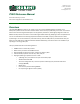
300 Henley Court Pullman, WA 99163 509.334.6306 www.digilentinc.com ZYBO Reference Manual Revised February 14, 2014 This manual applies to the ZYBO rev. B Overview The ZYBO (ZYnq BOard) is a feature-rich, ready-to-use, entry-level embedded software and digital circuit development platform built around the smallest member of the Xilinx Zynq-7000 family, the Z-7010.
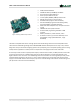
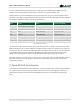
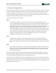
ZYBO™ FPGA Board Reference Manual Figure 1. ZYBO Zynq-7000 development board. ZYNQ XC7Z010-1CLG400C 512MB x32 DDR3 w/ 1050Mbps bandwidth Dual-role (Source/Sink) HDMI port 16-bits per pixel VGA source port Trimode (1Gbit/100Mbit/10Mbit) Ethernet PHY MicroSD slot (supports Linux file system) OTG USB 2.
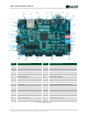
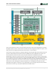
ZYBO™ FPGA Board Reference Manual 28 6 27 25 26 24 23 22 21 20 1 19 2 3 18 4 5 17 6 16 7 15 8 9 10 11 13 12 14 Callout Component Description Callout Component Description 1 Power Switch 15 Processor Reset Pushbutton 2 Power Select Jumper and battery header 16 Logic configuration reset Pushbutton 3 Shared UART/JTAG USB port 17 Audio Codec Connectors 4 MIO LED 18 Logic Configuration Done LED 5 MIO Pushbuttons (2) 19 Board Power Good LED 6 MIO Pmod 20 JTAG Port
ZYBO™ FPGA Board Reference Manual 1 Power Supplies The ZYBO can be powered from the Digilent USB-JTAG-UART port (J11), or from an external power supply. Jumper JP7 (near the power switch) determines which power source is used. There are three valid configurations for this jumper corresponding to the three powering options: USB, wall wart with barrel jack, and battery pack. There is a diagram on the board silkscreen indicating all three.
ZYBO™ FPGA Board Reference Manual minimum voltage of the battery pack depends on the application: if the USB Host (J10) or HDMI Source (J8) function is used, at least 4.6V need to be provided. In other cases the minimum voltage is 3.6V. Voltage regulator circuits from Analog Devices create the required 3.3V, 1.8V, 1.5V, and 1.0V supplies from the main power input.
ZYBO™ FPGA Board Reference Manual Figure 3. Zynq AP SoC architecture. The PL is nearly identical to a Xilinx 7-series Artix FPGA, except that it contains several dedicated ports and buses that tightly couple it to the PS. The PL also does not contain the same configuration hardware as a typical 7-series FPGA, and it must be configured either directly by the processor or via the JTAG port.
ZYBO™ FPGA Board Reference Manual There are many aspects of the Zynq AP SoC architecture that are beyond the scope of this document. For a complete and thorough description, refer to the Zynq Technical Reference Manual, available at www.xilinx.com. Figure 3 depicts the external components connected to the MIO pins of the ZYBO. The Zynq Board Definition File found on the Digilent ZYBO product page can be imported into EDK and Vivado Designs to properly configure the PS to work with these peripherals.
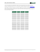
ZYBO™ FPGA Board Reference Manual MIO 501 1.8V Peripherals Pin ENET 0 16 TXCK 17 TXD0 18 TXD1 19 TXD2 20 TXD3 21 TXCTL 22 RXCK 23 RXD0 24 RXD1 25 RXD2 26 RXD3 27 RXCTL USB 0 28 DATA4 29 DIR 30 STP 31 NXT 32 DATA0 33 DATA1 34 DATA2 35 DATA3 36 CLK 37 DATA5 38 DATA6 39 DATA7 SDIO 0 40 CCLK 41 CMD 42 D0 43 D1 44 D2 45 D3 46 UART 1 GPIO RESETN 47 CD 48 RXD 49 TXD 50 BTN4 51 BTN5 52 MDC 53 MDIO Table 3. MIO Pinout.
ZYBO™ FPGA Board Reference Manual 3 Zynq Configuration Unlike Xilinx FPGA devices, AP SoC devices such as the Zynq-7010 are designed around the processor, which acts as a master to the programmable logic fabric and all other on-chip peripherals in the processing system. This causes the Zynq boot process to be more similar to that of a microcontroller than an FPGA.
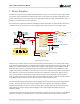
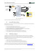
ZYBO™ FPGA Board Reference Manual USB-JTAG/UART Port Micro-AB USB Connector (J11) 6-pin JTAG Header (J12) Zynq USB Controller 1x6 JTAG Header JP6 MIO2/M3 JTAG Port Mode (JP5) MIO3/M1 MIO4/M2 MIO5/M0 MIO6/M4 MIO7/VCFG0 JP4 JP5 MIO8/VCFG1 MicroSD PROGRAM_B DONE PS_SRST_B QSPI Flash JTAG Programming Mode Figure 4. ZYBO configuration pins. The three boot modes are described in the following sections. 3.
ZYBO™ FPGA Board Reference Manual 3.3 JTAG Boot Mode When placed in JTAG boot mode, the processor will wait until software is loaded by a host computer using the Xilinx tools. After software has been loaded, it is possible to either let the software begin executing, or step through it line by line using Xilinx SDK. The ZYBO Base System Design includes a tutorial for debugging software over JTAG in Xilinx SDK. It is also possible to directly configure the PL over JTAG, independent of the processor.
ZYBO™ FPGA Board Reference Manual The PS incorporates an AXI memory port interface, a DDR controller, the associated PHY, and a dedicated I/O bank. DDR3 memory interface speeds up to 533 MHz/1066 Mbps are supported1. The DDR3 uses 1.5V SSTL-compatible inputs. The two components are organized in a tree topology with a series termination scheme while keeping traces as short as possible and matched.
ZYBO™ FPGA Board Reference Manual 2 Micro-USB (J11) 4 JTAG JTAG TXD RXD MIO48 MIO49 Zynq-7 TX LED LD9 LD8 RX LED FT2232 Figure 5. USB-UART bridge. Two on-board status LEDs provide visual feedback on traffic flowing through the port: the transmit LED (LD9) and the receive LED (LD8). Signal names that imply direction are from the point-of-view of the DTE (Data Terminal Equipment), in this case the PC.
ZYBO™ FPGA Board Reference Manual 1.8V CD DAT2 DAT3 CMD VDD CLK GND DAT0 DAT1 SD MICRO 3.3V SD_D2 SD_D3 SD_CMD MIO47 MIO44 MIO45 MIO41 SD_CCLK MIO40 SD_D0 SD_D1 MIO42 MIO43 TXS02612RTWR Zynq-7 Voltage Level Translator Figure 6. MicroSD slot signals. Both low speed and high speed cards are supported, the maximum clock frequency being 50 MHz. A Class 4 card or better is recommended. Refer to section 3.1 for information on how to boot from an SD card.
ZYBO™ FPGA Board Reference Manual management. The auxiliary interrupt (INTB) and reset (PHYRSTB) signals connect to PL pins to be accessed via EMIO. The connection diagram can be seen on Fig. 7. After power-up the PHY starts with Auto Negotiation enabled, advertising 10/100/1000 link speeds and full duplex. If there is an Ethernet-capable partner connected, the PHY automatically establishes a link with it, even with the Zynq not configured.
ZYBO™ FPGA Board Reference Manual MIO bank is powered from 1.8V, the RGMII interface uses 1.8V HSTL Class 1 drivers. For this I/O standard an external reference of 0.9V is provided in bank 501 (PS_MIO_VREF). Mapping out the correct pins and configuring the interface is handled by the ZYBO board definition file. Although the default power-up configuration of the PHY might be enough in most applications, the MDIO bus is available for management. The RTL8211E-VL is assigned address 00001b.
ZYBO™ FPGA Board Reference Manual When operating as Sink, the DDC function is required to be implemented so that a connected Source can read out important characteristics of the device. This can be done by emulating an I 2C-capable EEPROM in programmable logic. Likewise, in Source mode DDC can be used to find out the capabilities of the connected display. The HDMI/DVI protocol uses TMDS (Transition-minimized differential signaling) as I/O standard.
ZYBO™ FPGA Board Reference Manual 11.1 VGA System Timing VGA signal timings are specified, published, copyrighted, and sold by the VESA organization (www.vesa.org). The following VGA system timing information is provided as an example of how a VGA monitor might be driven in 640 by 480 mode. NOTE: For more precise information, or for information on other VGA frequencies, refer to documentation available at the VESA website.
ZYBO™ FPGA Board Reference Manual pattern, horizontally from left to right and vertically from top to bottom, as shown in Fig. 10. As the cathode ray moves over the surface of the display, the current sent to the electron guns can be increased or decreased to change the brightness of the display at the cathode ray impact point.
ZYBO™ FPGA Board Reference Manual A VGA controller circuit must generate the HS and VS timings signals and coordinate the delivery of video data based on the pixel clock. The pixel clock defines the time available to display one pixel of information. The VS signal defines the “refresh” frequency of the display, or the frequency at which all information on the display is redrawn.
ZYBO™ FPGA Board Reference Manual 12 Clock Sources The ZYBO provides a 50 MHz clock to the Zynq PS_CLK input, which is used to generate the clocks for each of the PS subsystems. The 50 MHz input allows the processor to operate at a maximum frequency of 650 MHz and the DDR3 memory controller to operate at a maximum of 525 MHz (1050 Mbps). The ZYBO Base System Design configures the PS to work properly with this input clock, and should be used as a reference when creating custom designs.
ZYBO™ FPGA Board Reference Manual PS 3.3V MIO Buttons MIO51 BTN5 MIO7 MIO LED LD12 MIO50 BTN4 3.3V Buttons PL Y16 BTN3 V16 BTN2 P16 BTN1 LEDs R18 BTN0 D18 G14 M15 M14 3.3V Slide Switches SW3 T16 SW2 W13 SW1 P15 SW0 G15 LD3 LD2 LD1 LD0 Zynq Figure 14. ZYBO GPIO. The high-efficiency LEDs are anode-connected to the Zynq via 330-ohm resistors, so they will turn on when a logic high voltage is applied to their respective I/O pin.
ZYBO™ FPGA Board Reference Manual The digital interface of the SSM2603 is wired to the programmable logic side of the Zynq. Audio data is transferred via the I2S protocol. Configuration is done over an I2C bus. The device address of the SSM2603 is 0011010b. All digital I/O are 3.3V level and connect to a 3.3V-powered FPGA bank.
ZYBO™ FPGA Board Reference Manual To use the audio codec in a design with non-default settings, it needs to be configured over I2C. The audio path needs to be established by configuring the (de)multiplexers and amplifiers in the codec. Some digital processing can also be done in the codec. Configuration is read out and written by accessing the register map via I 2C transfers. The register map is described in the SSM2603 datasheet. 15 Reset Sources 15.
ZYBO™ FPGA Board Reference Manual Pmod JA (XADC) Pmod JB (Hi-Speed) Pmod JC (Hi-Speed) Pmod JD (Hi-Speed) Pmod JE (Std.
ZYBO™ FPGA Board Reference Manual digital converter inside the Zynq (XADC). Any or all pairs in the connector can be configured either as analog input or digital input-output. In analog input mode, the voltage on these pins must be limited to 1V peak-to-peak. In digital mode, the regular VCCO-dependent limits apply. See Xilinx datasheets for more information. The Dual Analog/Digital Pmod on the ZYBO differs from the rest in the routing of its traces.