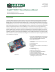
300 Henley Court Pullman, WA 99163 509.334.6306 www.digilentinc.com ChipKIT™WF32™ Board Reference Manual Revised September 16, 2013 This manual applies to Rev B of the board. Overview The chipKIT WF32 is based on the popular Arduino™ open-source hardware prototyping platform and adds the performance of the Microchip PIC32 microcontroller. The WF32 is the first board from Digilent to have a WiFi MRF24 and SD card on the board both with dedicated signals.
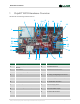
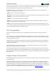
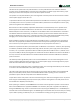
WF32 Reference Manual 1 ChipKIT WF32 Hardware Overview The WF32 has the following hardware features: 3 2 5 6 4 8 7 9 10 12 11 13 1 29 14 28 27 26 15 16 17 25 18 24 21 23 22 20 19 Call Out Component Description Call Out Component Description 1 IC3- Microchip MRF24WG0MA WiFi Module 16 J13- USB Connectors 2 User Buttons 17 JP9- USB Overcurrent Detect 3 JP3- Microchip Debug Tool Connector 18 JP11- Hos USB Bus Power Enable 19 J8- Analog and Digital Signal Connector 20
WF32 Reference Manual 11 12 13 14 15 J7- Digital Signal Connector User LEDs JP6,7- SPI Master/ SPI Slave Select J10- SPI Connector 26 J14- External Power Connector 27 J2- USB- UART Handshaking Signals 28 USB connector for USB Serial Converter 29 Serial Communication LEDs JP10- USB Host or OTG Select 2 MPIDE and USB Serial Communications The WF32 board is designed to be used with the Multi-Platform IDE (MPIDE), the MPIDE development platform was created by modifying the Arduino™ IDE.
WF32 Reference Manual attach the power supply to either J14 or J17 and place a shorting block in the EXT position of J15. Be sure to observe correct polarity when connecting a power supply to J14, as a reversed connection could damage the board. To operate the WF32 as a USB powered device from the USB OTG connector (J12) place a shorting block on the USB position of J15. This will normally only be done when running a sketch on the board that programs it to operate as a USB device.
WF32 Reference Manual LDO In is the input to the on-board linear regulator. LDO Out is the output of the on-board linear regulator VU is the unregulated input voltage selected by the jumper setting jumper block J15. 5V0 is the connection to the VCC5V0 power bus on the WF32 board. EN Ext is a signal provided to enable an external voltage regulator if one is being used. This would allow the sketch running on the WF32 to turn on/off the external voltage regulator.
WF32 Reference Manual powered from the VCC3V3 bus. No circuitry on the WF32 board is powered from the VCC5V0 power bus, leaving all current available from the 5V regulator to power external circuitry. The POWER connector (J3) is used to power shields connected to the WF32 board. Pin 1 is unconnected, the following pins are provided on this connector: IOREF (pin 2): This pin is tied to the VCC3V3 bus.
WF32 Reference Manual Note that the series resistors that are part of the voltage clamp circuit to provide 5V tolerance on the analog capable I/O pins, limiting the current that can be sourced or sunk by those pins. These resistors add 200 ohms of resistance to the input/output circuit and limit the effective drive current to about 1mA-2mA source/sink capability on the analog capable pins. Connectors J7 and J9 are 2x8 female pin header connectors that provide digital I/O signals.
WF32 Reference Manual The interface signals to the WiFi module are controlled by the network libraries and are not normally accessed by the user sketch. Refer to the schematic for the WF32 board for details on these connections. More detailed information about the operation of the MRF24WG0MA can be obtained from the manufacturer data sheet available from www.microchip.com.
WF32 Reference Manual The WF32 can be operated as a self-powered device or as a bus powered device from either the USB serial connector (J1) or the USB OTG/device connector (J12). As described in the power supply section above, jumper block (J15) is used to select the power source to be used to power the board. For operation as a self-powered device, place a shorting block on the EXT position of J15 and connect a suitable external power supply to either J14 or J17.
WF32 Reference Manual The VBUSON pin drives the enable input of a TPS2051B Current-Limited Power Distribution Switch to control the application of USB power to the host connector. This switch has over-current detection capability and provides an over-current fault indication by pulling the signal USBOC low. The over-current output pin can be monitored via the INT3/RA14 pin on the PIC32MX695 microcontroller. This signal appears on connector J7, pin 1 on the board, and is chipKIT digital pin 8.
WF32 Reference Manual 10.3 SPI Synchronous serial port. Pin 10 (SS), Pin 11 (MOSI), Pin 12 (MISO), Pin 13 (SCK).This can be accessed using the SPI standard library. It can also be accessed using the DSPI0 object from the DSPI standard library. This uses SPI2 (SS2, SDI2, SDO2, SCK2) on the PIC32 microcontroller. These signals also appear on connector J10.
WF32 Reference Manual 10.6 External Interrupts Pin 3 (INT0), Pin 2 (INT1), Pin 7 (INT2), Pin 8 (INT3), Pin 57 (INT4). Note that the pin numbers for INT0 and INT4 are different than on some other chipKIT boards. INT4 is dedicated for use with the MRF24WG0MA WiFi module and is not brought out to a connector pin. 10.7 User LEDs Pin 13 (LD6), Pin 43 (LD5), Pin 47 (LD4), Pin 48 (LD3). Pin 13 is shared between a connector pin and the LED. Pin 43, 48, and 47 only goes to the LED and not to any connector pin.
WF32 Reference Manual On Arduino boards, the corresponding connector is also used as an in-system programming connector as well as providing access to some of the SPI signals. On Arduino boards, pin 5 of this connector is connected to the reset net. Some Arduino shields, most notably the Ethernet shield, connect pin 5 to the reset net on pin 3 of connector J3. This causes the processor to be reset each time an attempt is made to access the SPI port.
WF32 Reference Manual alternate position for JP3 is the SS position. The digital pin number for the microcontroller signal SS is 44. With JP3 in the SS position, digital pin 44 is connected to the pin labeled 10 on the board, and digital pin 10 is not connected. The pin labeled 10 on the board is connected to connector J7 pin 5. This is shown as J5-05 in the following tables. In the ‘Pinout Table by Shield Connector Pin’ table below, J5-05 is shown has being either chipKIT pin # 10 or 44.
WF32 Reference Manual 24/A10 43 RB14 AN14/ERXD2/AETXD3/PMALH/PMA1/RB14 AIN10, GPIO 25/A11 44 RB15 AN15/ERXD3/AETXD2/OCFB/PMALL/PMA0/CN12/RB15 AIN11, GPIO 26 93 RE00 PMD0/RE0 GPIO 27 94 RE01 PMD1/RE1 GPIO 28 98 RE02 PMD2/RE2 GPIO 29 99 RE03 PMD3/RE3 GPIO 30 100 RE04 PMD4/RE4 GPIO 31 3 RE05 PMD5/RE5 GPIO 32 4 RE06 PMD6/RE6 GPIO 33 5 RE07 PMD7/RE7 GPIO 34 82 RD05 PMRD/CN14/RD5 GPIO 35 71 RD11 EMDC/AEMDC/IC4/PMCS1/PMA14/RD11 GPIO 36 83 RD06 ETXEN/PM
WF32 Reference Manual 59 90 RG00 PMD8/RG0 MRF24 RESET 60 41 RB12 AN12/ERXD0/AECRS/PMA11/RB12 power supply input voltage monitor 61 42 RB13 AN13/ERXD1/AECOL/PMA10/RB13 62 60 RA04 TDI/RA4 I2C Pullup (SDA) 63 61 RA05 TDO/RA5 I2C Pullup (SCL) 64 80 RD13 ETXD3/PMD13/CN19/RD13 5V Power Enable 65 91 RA06 TRCLK/RA6 BTN1 66 92 RA07 TRD3/RA7 BTN2 67 6 RC01 T2CK/RC1 68 7 RC02 T3CK/RC2 69 8 RC03 T4CK/RC3 70 68 RD08 RTCC/EMDIO/AEMDIO/IC1/RD8 71 69 RD09 SS1/IC2/RD
WF32 Reference Manual N/A 46 VDD POWER N/A 54 VBUS POWER N/A 55 VUSB POWER N/A 62 VDD POWER N/A 65 VSS POWER N/A 75 VSS POWER N/A 85 VCAP/VDDCORE POWER N/A 86 VDD POWER Pinout Table by MCU Port and Bit Port Bit MCU Pin ChipKIT Pin # PIC32 Signal Name Function RA00 17 47 TMS/RA0 User LED LD3 RA01 38 48 TCK/RA1 User LED LD4 RA02 58 45 SCL2/RA2 RA03 59 46 SDA2/RA3 RA04 60 62 TDI/RA4 I2C Pullup (SDA) RA05 61 63 TDO/RA5 I2C Pullup (SCL) RA06 91 6
WF32 Reference Manual RB09 33 22/A8 AN9/C2OUT/RB9 AIN8, GPIO RB10 34 18/A4 AN10/CVrefout/PMA13/RB10 AIN4, GPIO RB11 35 19/A5 AN11/ERXERR/AETXERR/PMA12/RB11 AIN5, GPIO RB12 41 60 AN12/ERXD0/AECRS/PMA11/RB12 power supply input voltage monitor RB13 42 61 AN13/ERXD1/AECOL/PMA10/RB13 RB14 43 24/A10 AN14/ERXD2/AETXD3/PMALH/PMA1/RB14 AIN10, GPIO RB15 44 25/A11 AN15/ERXD3/AETXD2/OCFB/PMALL/PMA0/CN12/RB15 AIN11, GPIO RC01 6 67 T2CK/RC1 RC02 7 68 T3CK/RC2 RC03 8 69 T4CK/RC
WF32 Reference Manual RE01 94 27 PMD1/RE1 GPIO RE02 98 28 PMD2/RE2 GPIO RE03 99 29 PMD3/RE3 GPIO RE04 100 30 PMD4/RE4 GPIO RE05 3 31 PMD5/RE5 GPIO RE06 4 32 PMD6/RE6 GPIO RE07 5 33 PMD7/RE7 GPIO RE08 18 2 AERXD0/INT1/RE8 GPIO, external INT RE09 19 7 AERXD1/INT2/RE9 GPIO, external INT, USBOC INT RF00 87 43 ETXD1/PMD11/RF0 User LED LD5 RF01 88 4 ETXD0/PMD10/RF1 GPIO RF02 52 0 SDA3/SDI3/U1RX/RF2 GPIO, UART RF03 51 N/A USBID/RF3 P32_USBID RF04 49
WF32 Reference Manual 31 N/A AVSS POWER 36 N/A VSS POWER 37 N/A VDD POWER 45 N/A VSS POWER 46 N/A VDD POWER 54 N/A VBUS POWER 55 N/A VUSB POWER 62 N/A VDD POWER 65 N/A VSS POWER 75 N/A VSS POWER 85 N/A VCAP/VDDCORE POWER 86 N/A VDD POWER Pinout Table by PIC32 Microcontroller Pin MCU Pin Port Bit ChipKIT Pin # PIC32 Signal Name Function 1 RG15 49 AERXERR/RG15 SD Card N/A VDD POWER 2 3 RE05 31 PMD5/RE5 GPIO 4 RE06 32 PMD6/RE6 GPIO 5 RE07
WF32 Reference Manual GPIO, external INT 18 RE08 2 AERXD0/INT1/RE8 19 RE09 7 AERXD1/INT2/RE9 20 RB05 21/A7 AN5/C1IN+/VBUSON/CN7/RB5 21 RB04 15/A1 AN4/C1IN-/CN6/RB4 AIN1, GPIO 22 RB03 20/A6 AN3/C2IN+/CN5/RB3 AIN6, GPIO 23 RB02 14/A0 AN2/C2IN-/CN4/RB2 AIN0, GPIO 24 RB01 23/A9 PGEC1/AN1/CN3/RB1 AIN9, GPIO 25 RB00 17/A3 PGED1/AN0/CN2/RB0 AIN3, GPIO 26 RB06 N/A PGEC2/AN6/OCFA/RB6 ICSP 27 RB07 N/A PGED2/AN7/RB7 ICSP 28 RA09 41 Vref-/CVref-/AERXD2/PMA7/RA9 GPIO,
WF32 Reference Manual 54 N/A VBUS POWER 55 N/A VUSB POWER 56 RG03 N/A D-/RG3 P32_USBD- 57 RG02 N/A D+/RG2 P32_USBD+ 58 RA02 45 SCL2/RA2 59 RA03 46 SDA2/RA3 60 RA04 62 TDI/RA4 I2C Pullup (SDA) 61 RA05 63 TDO/RA5 I2C Pullup (SCL) N/A VDD POWER 62 I2C, wire (jumper to A5) I2C, wire (jumper to A4) 63 RC12 N/A OSC1/CLKI/RC12 XTAL 64 RC15 N/A OSC2/CLKO/RC15 XTAL N/A VSS POWER 65 66 RA14 8 AETXCLK/SCL1/INT3/RA14 GPIO, external INT (shared with P32_USBOC)
WF32 Reference Manual 86 N/A VDD POWER 87 RF00 43 ETXD1/PMD11/RF0 User LED LD5 88 RF01 4 ETXD0/PMD10/RF1 GPIO 89 RG01 58 ETXERR/PMD9/RG1 MRF24 HIBERNATE 90 RG00 59 PMD8/RG0 MRF24 RESET 91 RA06 65 TRCLK/RA6 BTN1 92 RA07 66 TRD3/RA7 BTN2 93 RE00 26 PMD0/RE0 GPIO 94 RE01 27 PMD1/RE1 GPIO 95 RG14 50 TRD2/RG14 SD Card 96 RG12 51 TRD1/RG12 SD Card 97 RG13 52 TRD0/RG13 SD Card 98 RE02 28 PMD2/RE2 GPIO 99 RE03 29 PMD3/RE3 GPIO 100 RE04 30 PMD4/
WF32 Reference Manual Declaration of Conformity In accordance with EN ISO/IEC 17050-1:2010 Manufacturers Name: Digilent, Inc. Manufacturers Address: 1300 NE Henley Court Pullman, WA 99163 U.S.A.