
Owner's manual
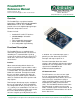

PmodGYRO™ Reference Manual
®
www.digilentinc.com
www.digilentinc.com Copyright Digilent, Inc. page 2 of 2
I
2
C Communication
The I
2
C standard uses two signal lines, I
2
C
data (SDA) and serial clock (SCL). The
device supports both standard, 100 kHz, and
fast, 400 kHz, serial clocks. In accordance
with I
2
C protocol, the L3G4200D has a device
specific 7-bit address used by the serial
master to communicate with multiple devices
on a data bus. The device uses the address
110100xb, where pin 3 on J1 (SDO/SA0)
defines the least-significant-bit (LSB). By
default, the LSB of the address while be ‘1’
due to a pull-up resistor on JP1 as shown by
the schematic available on the Digilent
website. While the default value is ‘1’, by
simply connecting pin 3 on J1 to the ground
rail the user can change the LSB to a ‘0’. This
user selectable bit enables two PmodGYROs
to be used on the same I
2
C bus. The data
sheet for the L3G4200D contains further
device specific I
2
C information.
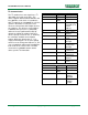
Connector J1
–
SPI Commun
ications
Pin
Signal
Description
1 CS Chip Select
2 SDA/SDI/
SDO
Serial Data In
3 SDO/SA0
Serial Data
Out/LSB of I
2
C
Device
Address
4 SCL/SPC Serial Clock
5 GND Power Supply
Ground
6 VCC Power Supply
(3.3V)
7 INT1 Programmable
Interrupt
8 INT2 Data
Ready/FIFO
Interrupt
9 NC Not
Connected
10 NC Not
Connected
11 GND Power Supply
Ground
12 VCC Power Supply
(3.3V)
Connector J2
–
I
2
C Communication
Pin
Signal
Description
1 & 2 SCL/SPC Serial Clock
3 & 4 SDA/SDI/
SDO
Serial Data
5 & 6 GND Power
Supply
Ground
7 & 8 VCC Power
Supply
(3.3V)